Metal-induced crystallization of amorphous silicon and metal removal techniques

An amorphous silicon film and technology technology, applied in semiconductor/solid-state device manufacturing, electrical components, circuits, etc., can solve problems affecting polysilicon crystallization quality and crystallization speed, affecting the final characteristics of TFT, etc.

Inactive Publication Date: 2007-10-31
THE HONG KONG UNIV OF SCI & TECH
View PDF7 Cites 10 Cited by
  • Summary
  • Abstract
  • Description
  • Claims
  • Application Information

AI Technical Summary

Problems solved by technology

However, the early occurrence of the gettering process will affect the crystallization quality and crystallization speed of polysilicon, and the gettering

Method used


Image

  • Metal-induced crystallization of amorphous silicon and metal removal techniques
  • Metal-induced crystallization of amorphous silicon and metal removal techniques
  • Metal-induced crystallization of amorphous silicon and metal removal techniques

Examples


specific Embodiment

[0042] The specific embodiment preparation method is:

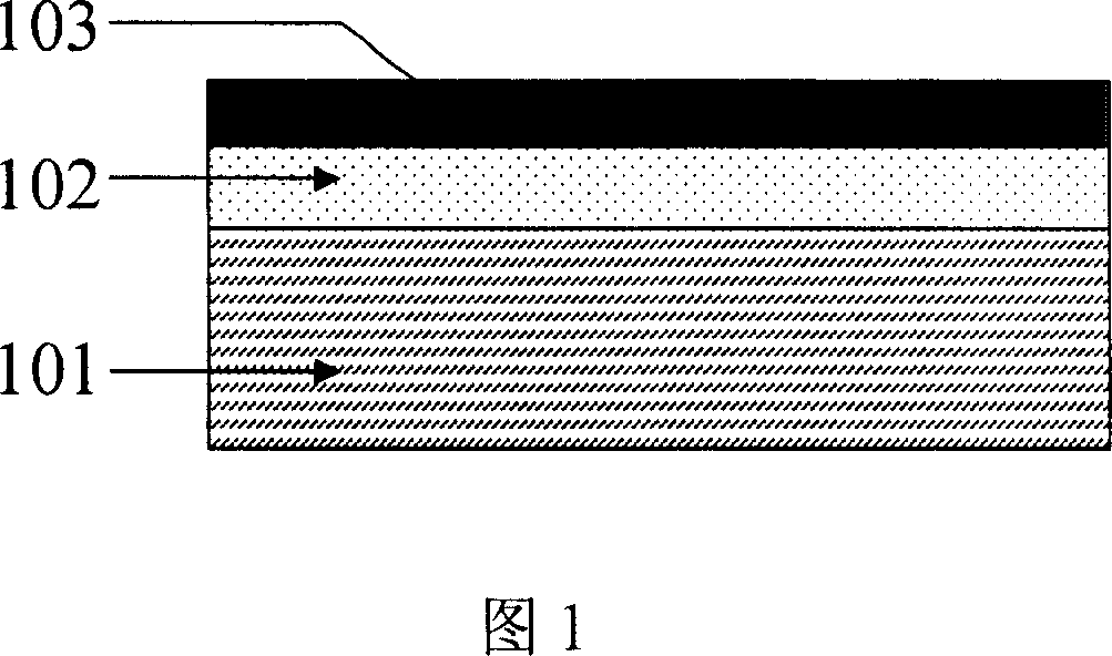
[0043] 1: 200 nanometers of silicon nitride and 100 nanometers of LTO are deposited as a barrier layer 102 on Corning 1737F glass 101 behind a thickness of 1.1 mm by PECVD. LPCVD at 550° C. to deposit a 50 nm amorphous silicon layer 103 .

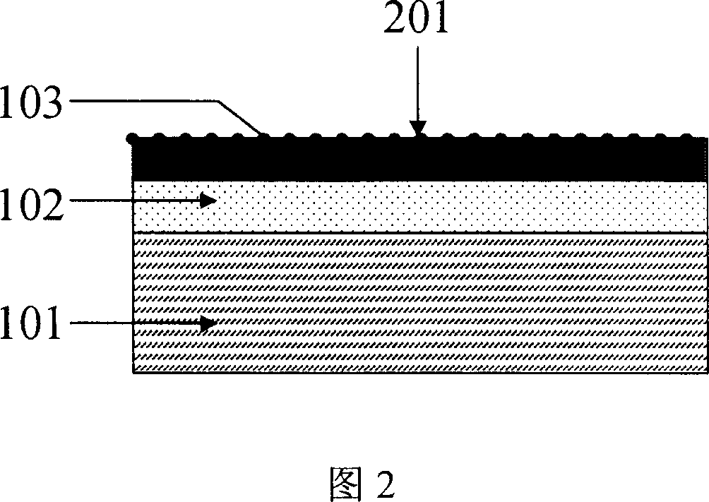
[0044] 2: Using a nickel-silicon mixed target, sputtering in an argon-oxygen atmosphere to achieve a small amount of nickel 201 attached to the surface of amorphous silicon.

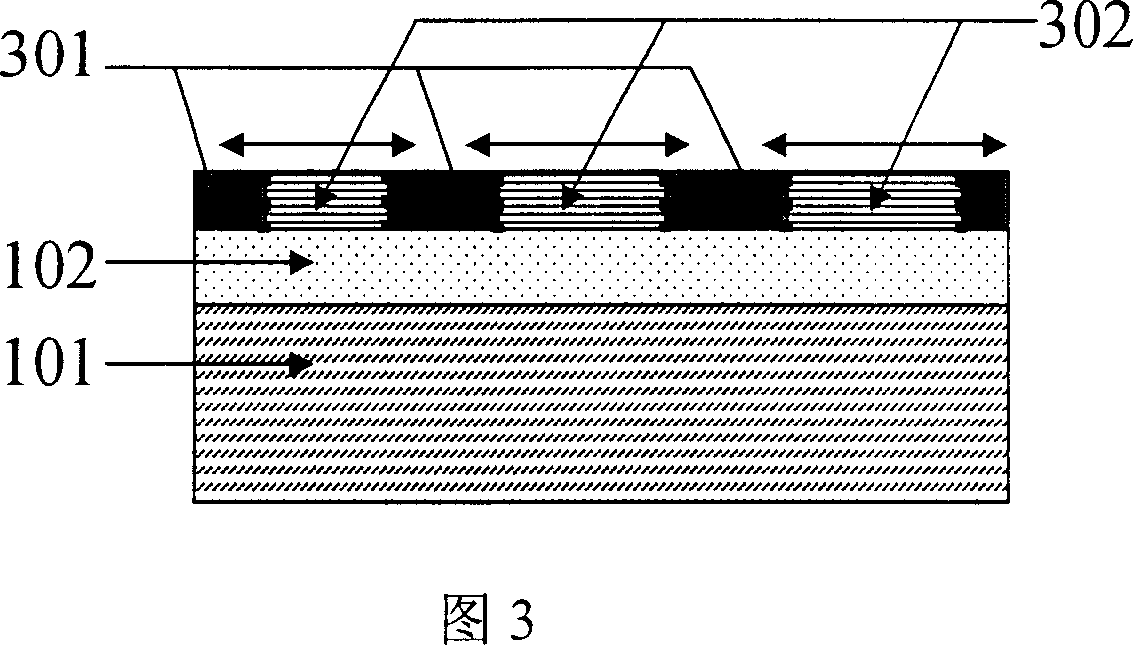
[0045] 3: The above samples were annealed in a nitrogen atmosphere at a temperature of 590° C. for 1 hour. It becomes a mixed film of the amorphous silicon film 301 and the polysilicon film 302 .

[0046] 4: Use diluted hydrofluoric acid to remove the natural oxide layer on the surface of the sample and clean the surface. Afterwards, LPCVD deposited PSG 501 with a thickness of 700 nm.

[0047] 5: The above sample is subjected to the second annealing process in a nitrogen atmosphere at a temperature of 590° C....


PUM

PropertyMeasurementUnit
Thicknessaaaaaaaaaa
Thicknessaaaaaaaaaa

Abstract

The invention relates to a technology for producing a high quality and large area polycrystalline silicon thin film by amorphous silicon-metal-induced crystallization. Crystallization-inducing metal elements of controllable amound are introduced onto an initial amorphous silicon thin film. A first, low-temperature, heat-treatment induces nucleation of metal-induced crystallization (MIC), resulting in the formation of small polycrystalline silicon''islands''. A metal-gettering layer is formed on the resulting partially crystallized thin film. A second, low-temperature, heat-treatment completes the MIC process to form the desired polycrystalline silicon thin film. while the metal-gettering layer can be removed at randon after crystallization heat-treatment.

Description

technical field [0001] The invention relates to the technology of preparing high-quality and large-area polysilicon film by inducing crystallization of amorphous silicon metal. This technique requires the introduction of controlled amounts of crystallization-inducing metal elements to the starting amorphous silicon film; the first low-temperature heat treatment causes metal-induced crystallization nucleation and the formation of small polysilicon "islands"; at this point the film material is partially crystallized The metal gettering layer is formed on it; the metal-induced crystallization process is completed in the second low-temperature heat treatment process, and the desired polysilicon film is formed; the metal gettering layer is removed after the crystallization heat treatment is completed. Background technique [0002] TFT can be applied to active matrix liquid crystal display, active matrix organic light emitting diode display, active matrix e-book and active matrix ...

Claims


Application Information

Patent Timeline
IPC IPC(8): H01L21/20H01L21/322H01L21/336H01L21/84
Inventor 王文郭海成孟志国张冬利施雪捷
Owner THE HONG KONG UNIV OF SCI & TECH
Why Eureka
Try Eureka