Method for realizing RTD and HEMT single chip integration using dry etching technology

A technology of dry etching and monolithic integration, which is applied in the direction of electrical components, semiconductor/solid-state device manufacturing, circuits, etc., and can solve the problems of not being suitable for industrialized mass production, not being suitable for small-sized device circuits, and being unable to accurately control device sizes, etc. problem, to achieve the effect that is beneficial to the consistency of threshold voltage and transconductance, good etching uniformity, and good directionality

Inactive Publication Date: 2007-10-31
INST OF SEMICONDUCTORS - CHINESE ACAD OF SCI
View PDF0 Cites 23 Cited by
  • Summary
  • Abstract
  • Description
  • Claims
  • Application Information

AI Technical Summary

Problems solved by technology

[0007] At present, the monolithic integration of RTD and HEMT is mainly realized by wet etching method. However, due to the common lateral corrosion in wet process, the size of the device cannot be accurately controlled, and it is not suitable for the production of small-sized device circuits.
Moreover, due to the consistency of the wet method, uniform corrosion cannot be achieved on the entire sheet (especially above 4 inches), which is not conducive to the integration of large-scale devices, and does not meet the needs of industrialized mass production.

Method used


Image

  • Method for realizing RTD and HEMT single chip integration using dry etching technology
  • Method for realizing RTD and HEMT single chip integration using dry etching technology
  • Method for realizing RTD and HEMT single chip integration using dry etching technology

Examples


Embodiment

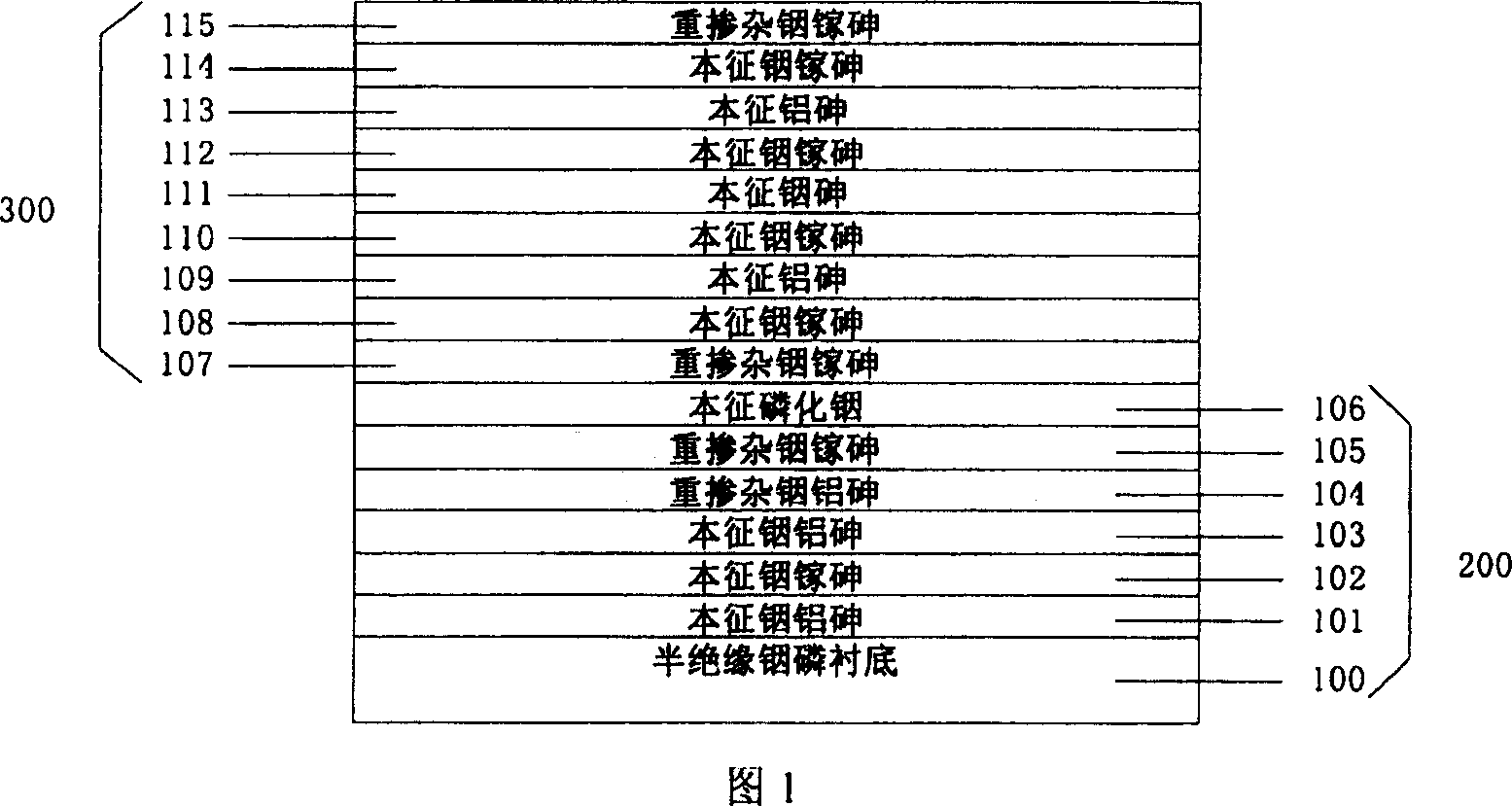
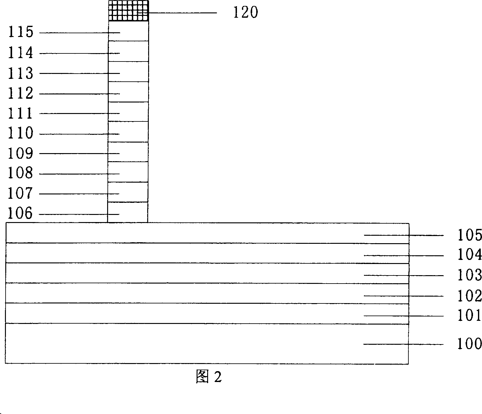
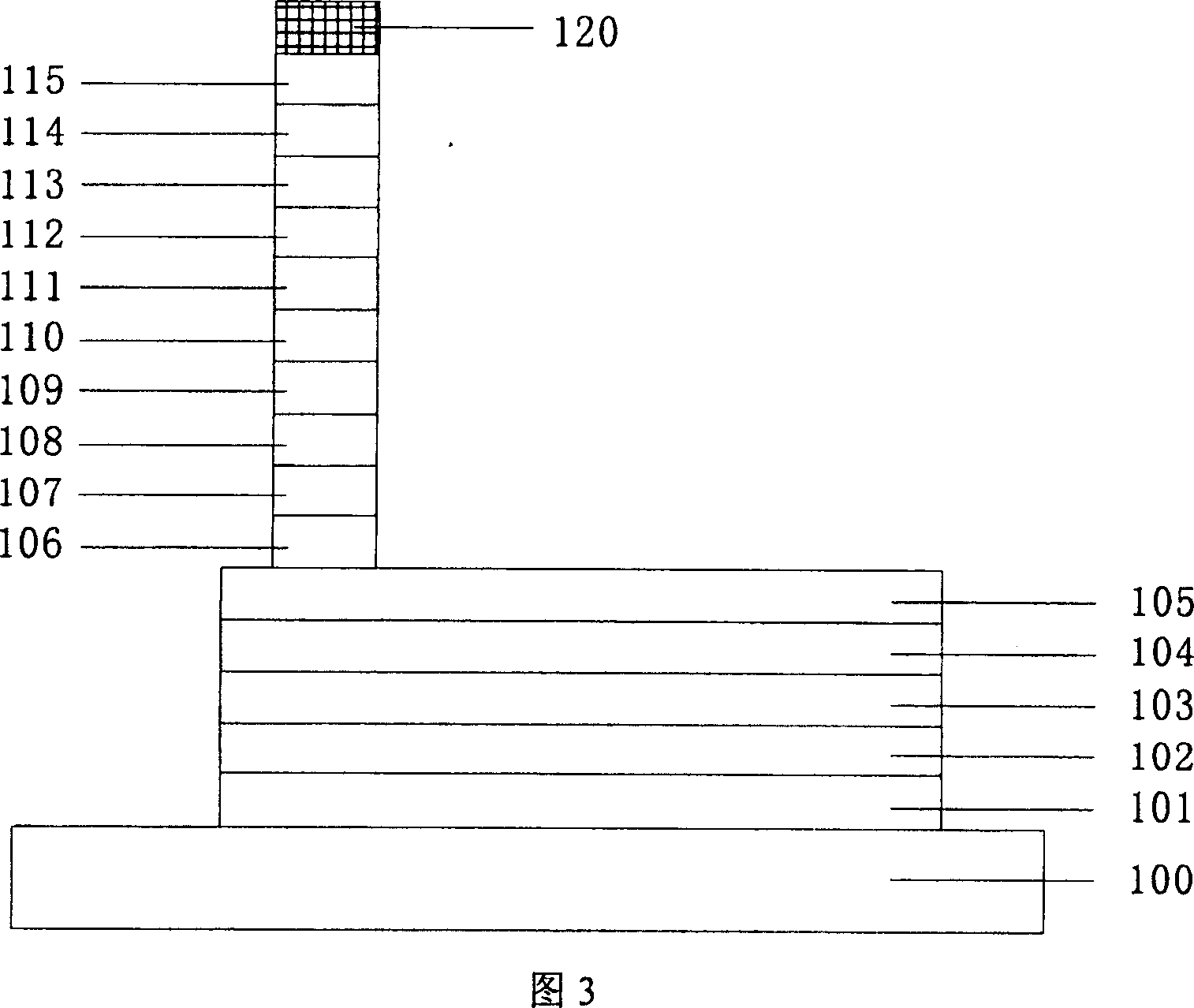
[0060] Please refer to Fig. 1-Fig. 9 again, a kind of method that adopts dry etching technology to realize RTD and HEMT monolithic integration of the present invention, comprises the following steps:

[0061] Step 1: On the semi-insulating InP substrate 100, the material structure of HEMT and RTD is sequentially grown by molecular beam epitaxy: the HEMT structure includes a 2000A non-doped InAlAs buffer layer 101, a 150A non-doped InGaAs channel 102, and a 30A non-doped Doped InAlAs isolation layer 103, 4×1012 cm-2 delta plane doped layer, 200A non-doped InAlAs barrier 104 and 200A heavily doped InGaAs cap layer 105. This is followed by a 50AInP selective etch stop layer 106, and an RTD structure including a heavily doped 500AInGaAs collector contact layer 107, a 50A undoped collector spacer 108, a 16A undoped AlAs barrier 109, and a 13A undoped Doped InGaAs well 110, 18A non-doped InAs sub-well 111, 13A non-doped InGaAs well 112, 16A non-doped AlAs barrier 113, 50A non-doped ...


PUM


Abstract

A method of realizing integrating of RTD and HEMT using dry etching technique includes: Vegetating typical HEMT material structure and RTD material structure on the underlay; photoengraving the pattern of RTD emitting area to produce AuGeNi metal layer to form RTD metal emitting pole; photoengraving to form source area; photoengraving the source electrode and drain electrode of HEMT; anneal in high temperature; photoengraving the HEMT bar pattern to corrode part of the adulteration hat layer; a layer of passivation medium is deposited on surface of device; photoengraving the HEMT gate electrode pattern to generate TiPtAu metal as the gate electrode of HEMT element; photoengraving the down-lead hole; photoengraving the down-lead interlinkage area, vaporizing or sputtering thick TiAlTiAu metal electrode, and then it is peeled off.

Description

technical field [0001] The invention belongs to the technical field of semiconductors, in particular to the technology of preparing resonant tunneling diodes and transistor monolithic integrated circuits on III-V substrates. Background technique [0002] Since the industrialized mass production of silicon large-scale integrated circuits in the 1960s, Moore's Law has been followed to improve circuit performance through the reduction of feature size, achieving higher integration, faster speed and lower power consumption. Because of this, at the end of the last century, Intel delivered Pentium processor chips and personal computers with unprecedented levels of integration and performance to users. At present, the characteristic size of MOSFET has reached 45nm, and then as the characteristic size approaches the nanometer scale, quantum effects gradually appear and dominate, and some problems such as metal interconnection, current tunneling and power consumption are becoming more...

Claims


Application Information

Patent Timeline
Patent Type & Authority Applications(China)
IPC IPC(8): H01L21/82H01L21/822H01L21/84
Inventor 马龙杨富华王良臣黄应龙
Owner INST OF SEMICONDUCTORS - CHINESE ACAD OF SCI
Why Eureka
Try Eureka