Eureka AIR delivers breakthrough ideas for toughest innovation challenges, trusted by R&D personnel around the world.

Method for compensating round angle of metal bump for semiconductor chip electric contact

A technology of metal bumps and compensation methods, which is applied in semiconductor devices, semiconductor/solid-state device manufacturing, circuits, etc., can solve problems such as corner deformation into rounded corners, and achieve the effects of quality improvement, easy implementation, and improved front appearance

Inactive Publication Date: 2007-11-14
CHIPMORE TECH CORP LTD
View PDF0 Cites 3 Cited by
  • Summary
  • Abstract
  • Description
  • Claims
  • Application Information

AI Technical Summary

Problems solved by technology

[0020] The invention provides a method for compensating rounded corners of metal bumps used for electrical contacts of semiconductor chips. The purpose of the method is to solve the problem that the corners of the metal bumps are deformed into rounded corners during the production process of the metal bumps, so that the corners of the bumps (bump) can be kept complete and regular. Corner shape to overcome lack of rounded corners

Method used


Image

  • Method for compensating round angle of metal bump for semiconductor chip electric contact
  • Method for compensating round angle of metal bump for semiconductor chip electric contact
  • Method for compensating round angle of metal bump for semiconductor chip electric contact

Examples


Embodiment 1

[0056] Embodiment 1: A method for rounding corner compensation of a rectangular gold bump. During the manufacturing process of a rectangular gold bump combined with photolithography and electroplating, the four theoretically designed corners of the bump pattern on the mask are turned outward Extend and increase the size of the window to make up for the defects caused by insufficient developer replenishment during the development process, that is, the inward shrinkage deformation produces rounded corners, so as to ensure that the corners of the actually produced gold bumps are right angles. There are four types of specific implementation methods:

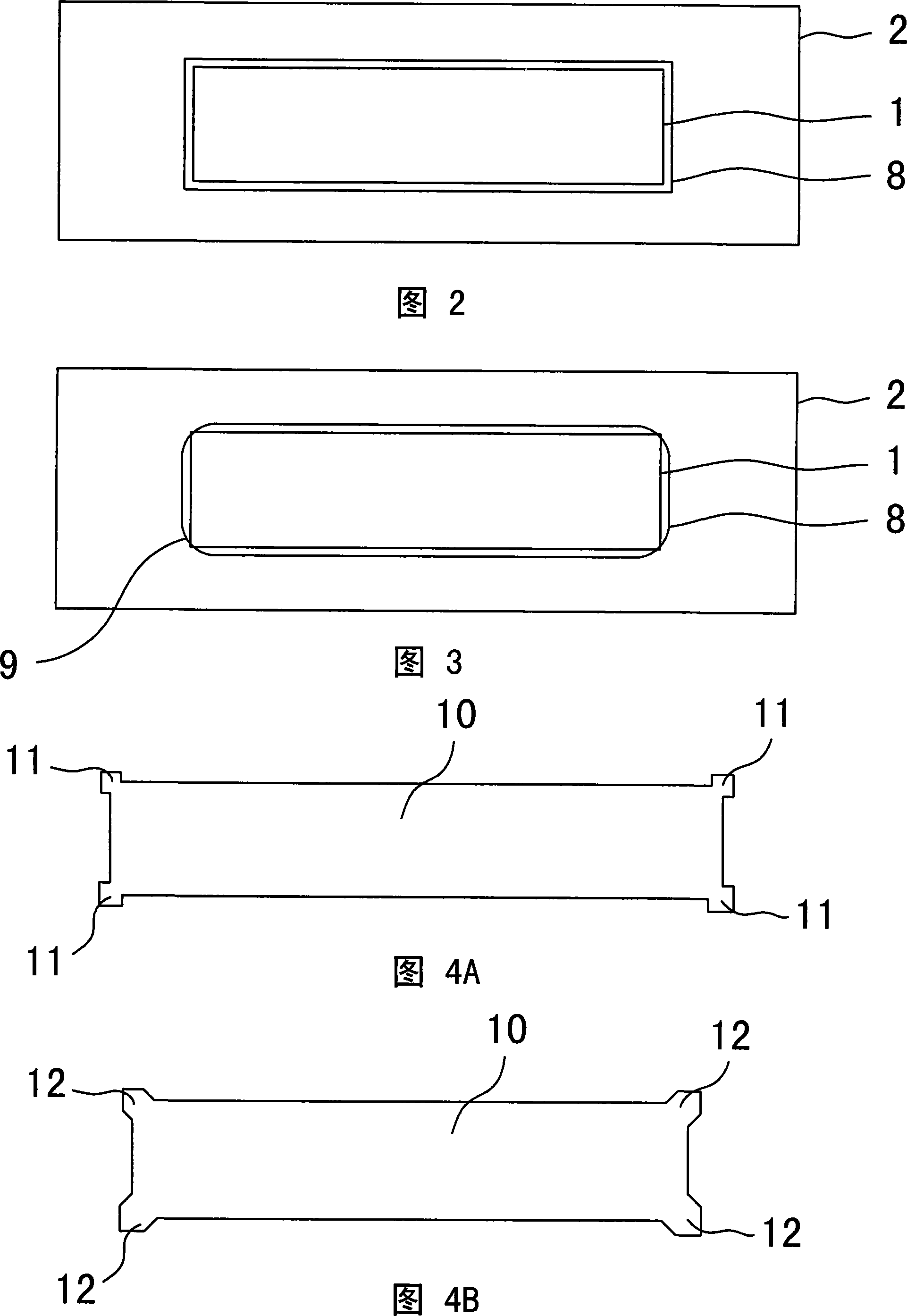
[0057] 1. As shown in FIG. 4A, in the mask design, the four right angles of the rectangular gold bump pane 10 are partially enlarged in proportion, and the compensation angle 11 is extended to the outside to increase the window size. The shape is shown in Figure 4A. The compensation angle 11 is still a right angle. Fig. 4B is anoth...

Embodiment 2

[0063] Embodiment 2: A method for round corner compensation of a prismatic gold bump, and the specific implementation methods include the following four types:

[0064] 1. As shown in FIG. 8 , in the mask design, the two acute angles of the prismatic gold bump pane 16 are partially enlarged proportionally, and the compensation angle 17 is extended outward to increase the window size. The two obtuse angles are partially enlarged in proportion, and a compensation angle 18 is extended to the outside to increase the size of the window.

[0065] 2. As shown in Figure 9, in the mask design, the two acute angles of the prismatic gold bump pane 16 are partially expanded outwards, and the compensation angle 19 is extended outwards to increase the size of the window, and the compensation angle 19 The angle is smaller than the theoretical design angle. The two obtuse angles adopt the method of local expansion to the outside, and extend the compensation angle 20 to the outside to increas...

Embodiment 3

[0068] Embodiment 3: As shown in FIG. 12 , a method for round corner compensation of a right-angled triangular gold bump, in the mask design, a right angle of the right-angled triangle pane 25 is partially enlarged in proportion to extend outward The compensation angle 26 increases the size of the window, and the compensation angle 26 is still a right angle. The two acute angles are locally enlarged in proportion, and the compensation angle 27 is extended to the outside to increase the size of the window. The angle of the compensation angle 27 is equal to the theoretical design angle.


PUM


Abstract

The invention is a semiconductor chip connection point metal bump round angle compensating method, characterized by: in the course of making metal bump by combination of photoetching and plating processes, extending outward each corner theoretically designed in bump figure on photomask, increasing windowing size and compensating the inward contraction distortion of the bump figure in developing so as to assure the actually made metal bump corner consistent with the geometric shape theoretically designed. And the invention relates to the field of semiconductor IC packaging technique, solving the problem that the corner deforms into round angle in the metal bump making course, optimizing bump angular shape and improving product performance and yield.

Description

technical field [0001] The invention relates to the technical field of packaging of semiconductor integrated circuits, in particular to a fillet compensation method for manufacturing metal bumps (bumps) for electrical contacts on aluminum pads (Al pads) of semiconductor chips. The method can improve the corner shape of the metal bump and avoid rounded corners, thereby optimizing the bump and improving product performance and pass rate. Background technique [0002] In the semiconductor industry, chip production is mainly divided into two stages: circuit fabrication and chip packaging and testing. In packaging and testing operations, one of the key steps is the bumping process. A typical metal bump manufacturing process includes the following basic steps: sputteringphotoresist application → exposure → development → electroplatingphotoresist removal → etchingtoughening. Among them, photoresist application, exposure, and development are photolithography processes. T...

Claims


Application Information

Patent Timeline
Patent Type & Authority Applications(China)
IPC IPC(8): H01L21/60
CPCH01L24/11H01L2224/11H01L2924/14H01L2924/00H01L2924/00012
Inventor 陈文勇许红飞
Owner CHIPMORE TECH CORP LTD
Why Eureka
Eureka Blog
Learn More