Implementation method for 3D integrated circuit

A technology of integrated circuits and implementation methods, applied in circuits, electrical components, electrical solid devices, etc., can solve problems such as hole sealing and restrict the development of three-dimensional integrated circuits, and achieve the effect of compact three-dimensional integrated circuits

Inactive Publication Date: 2007-11-28
TSINGHUA UNIV
View PDF0 Cites 16 Cited by
  • Summary
  • Abstract
  • Description
  • Claims
  • Application Information

AI Technical Summary

Problems solved by technology

However, since only Damascus electroplating can be used, it is easy to seal the hole first at the opening during the electroplating process, forming a hole inside the interconnection line.
Limit the application of this technology and the development of three-dimensional integrated circuits

Method used


Image

  • Implementation method for 3D integrated circuit
  • Implementation method for 3D integrated circuit
  • Implementation method for 3D integrated circuit

Examples


Embodiment Construction

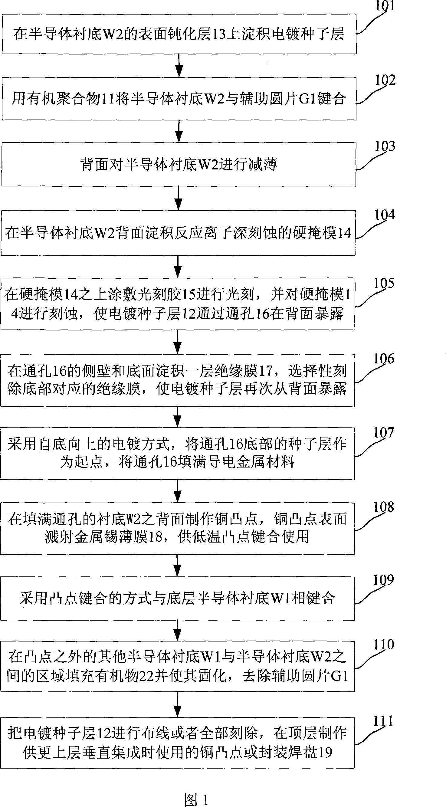
[0043] In order to make the object, technical solution and advantages of the present invention clearer, the implementation manner of the present invention will be further described in detail below in conjunction with the accompanying drawings.

[0044]Embodiments of the present invention provide a simple and feasible method for realizing a three-dimensional integrated circuit based on electroplating copper interconnection, which can effectively realize a very thin and very compact three-dimensional integrated circuit with a single layer.

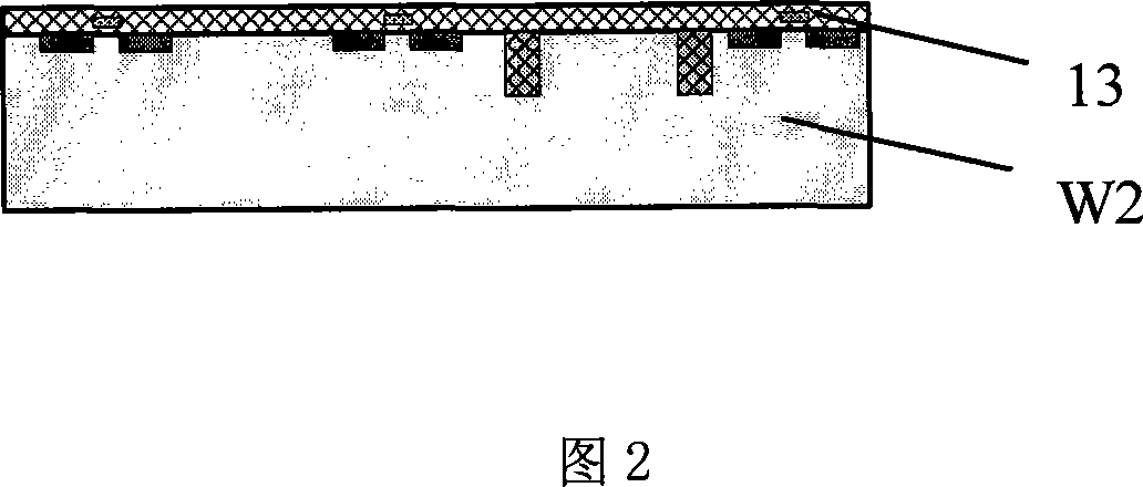
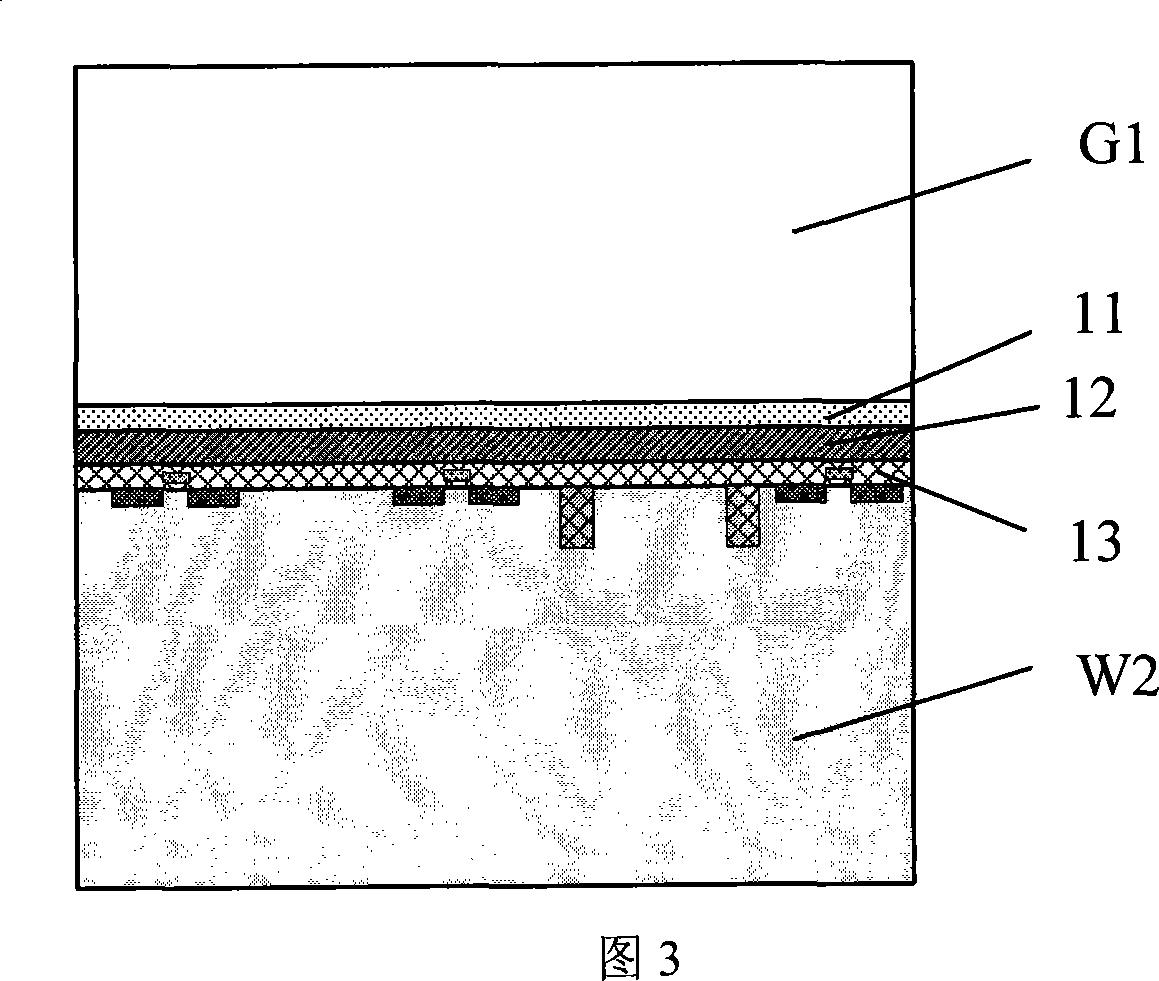
[0045] Referring to Fig. 1, the present embodiment provides a method for realizing a three-dimensional integrated circuit, referring to Fig. 2, which includes a semiconductor substrate W2 and a surface passivation layer 13 of the semiconductor substrate W2, wherein the semiconductor substrate material may be silicon , silicon germanium, gallium arsenide (GaAs), or silicon-on-insulator (SOI). Taking the circuit wafer provided in Figure 2 as a...


PUM


Abstract

The invention discloses a realizng method of three-dimensional integrated circuit in the semiconductor making technique and three-dimensional integrated technical domain, which comprises the following steps: sedimenting plating seed layer on the bonding face of the first circuit disc or auxiliary disc; making the auxiliary disc as the through-hole to reduce the back to support the first layer of circuit disc and etch the disc; exposing the plating seed layer through the through-hole; using plating technique from bottom to top; adopting the plating seed layer as original; plating to fill the through-hole; making projection on the filled through-hole; adopting bonding pattern to connect the first layer of circuit disc and the second layer of circuit disc. The invention reduces the technical difficulty to realize three-dimensional integration on the silicon substrate, which has good versatility.

Description

technical field [0001] The invention relates to the fields of semiconductor manufacturing technology and three-dimensional integration technology, in particular to a method for realizing a three-dimensional integrated circuit. Background technique [0002] The development of traditional integrated circuits basically follows Moore's law, and the degree of integration is constantly developing at a rate of doubling every 18 months. The continuous reduction of feature size and the continuous improvement of integration not only make the feature size of traditional integrated circuits gradually approach the physical limit, but also make integrated circuits encounter insurmountable development bottlenecks in terms of design, manufacturing and cost. [0003] The continuous reduction of CMOS (Complementary Metal-Oxide Semiconductor) devices has led to continuous improvement of integration. At present, more than 1 billion transistors can be integrated on a chip area per square centime...

Claims


Application Information

Patent Timeline
Patent Type & Authority Applications(China)
IPC IPC(8): H01L21/60
CPCH01L2224/16145
Inventor 王喆垚宋崇申蔡坚刘理天
Owner TSINGHUA UNIV
Why Eureka
Try Eureka