Tensile and compressive stressed materials for semiconductors

A technology of stress materials and tensile stress, which is applied in the direction of semiconductor devices, semiconductor/solid-state device manufacturing, metal material coating technology, etc., and can solve problems such as limitations

Inactive Publication Date: 2007-12-12
APPLIED MATERIALS INC
View PDF1 Cites 18 Cited by
  • Summary
  • Abstract
  • Description
  • Claims
  • Application Information

AI Technical Summary

Problems solved by technology

A reduction in supply voltage allows lower operating power levels...

Method used


Image

  • Tensile and compressive stressed materials for semiconductors
  • Tensile and compressive stressed materials for semiconductors
  • Tensile and compressive stressed materials for semiconductors

Examples


Embodiment Construction

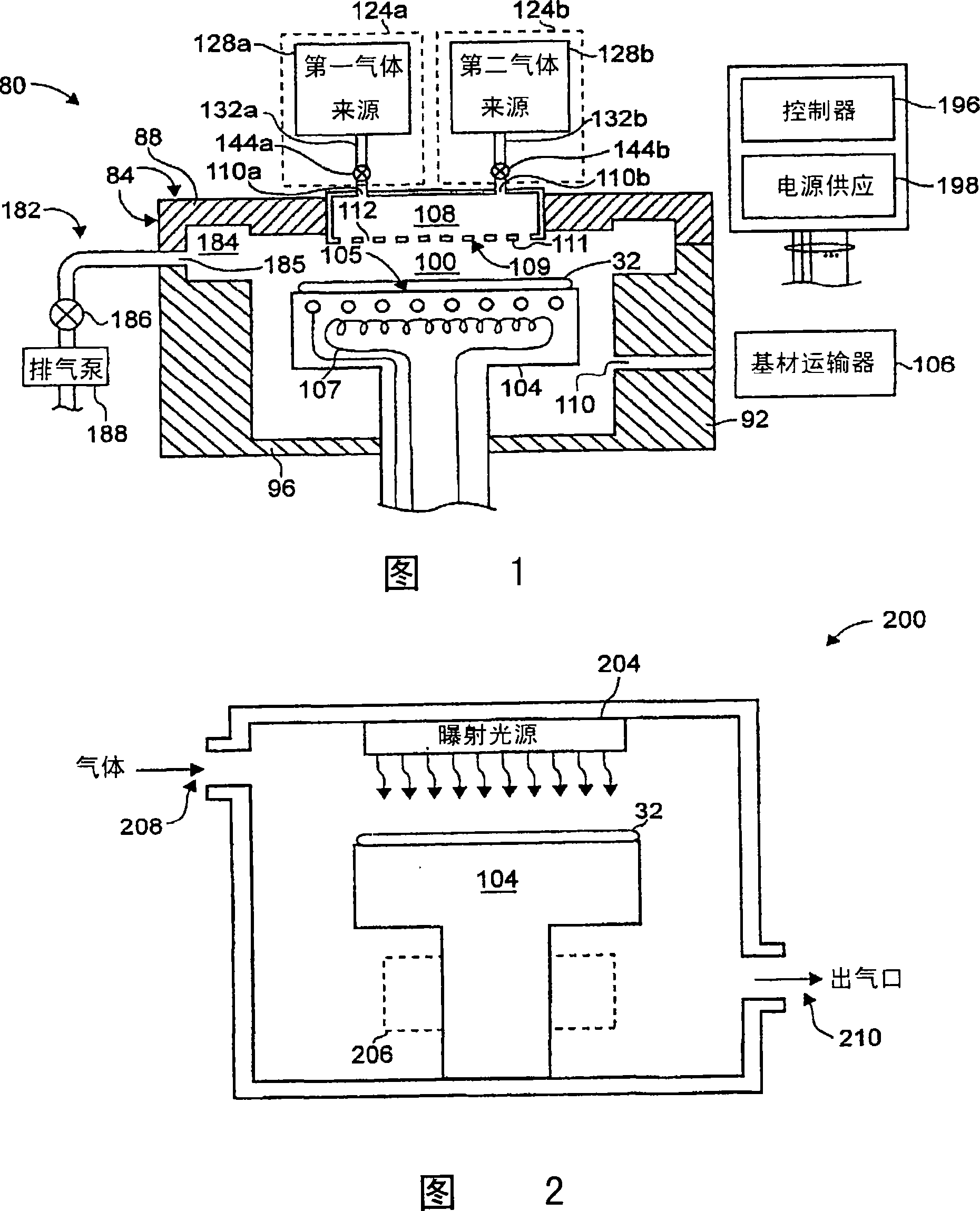
[0060] FIG. 1 schematically illustrates an embodiment of a substrate processing chamber 80 for depositing stressed materials in accordance with the present invention. This demonstration chamber is used to illustrate the invention, but other chambers may be used by those skilled in the art. Accordingly, the scope of the present invention should not be limited to the exemplary embodiment of the chamber or other features mentioned herein. Generally, the chamber 80 is used as a plasma-assisted chemical vapor deposition (PE-CVD) chamber for processing a substrate 32 (eg, a silicon wafer). For example, a suitable process chamber is the Producer manufactured by Applied Materials of Santa Clara, California, USA.  SE type room. The chamber 80 includes sealing walls 84 , including a top cover 88 , side walls 92 , and a bottom wall 96 , which seal off a processing zone 100 . The chamber 80 also includes a gasket (not shown) surrounding the processing zone 100 as a gasket for at least...


PUM


Abstract

A stressed film is formed on a substrate. The substrate is placed in a process zone and a plasma is formed of a process gas provided in the process zone, the process gas having silicon-containing gas and nitrogen-containing gas. A diluent gas such as nitrogen can also be added. The as-deposited stressed material can be exposed to ultraviolet radiation or electron beams to increase the stress value of the deposited material. In addition or in the alternative, a nitrogen plasma treatment can be used to increase the stress value of the material during deposition. Pulsed plasma methods to deposit stressed materials are also described.

Description

technical field [0001] The present invention relates generally to semiconductor technology, and more specifically to a method of depositing a stressed material on a substrate. Background technique [0002] During the fabrication of substrates for circuits and displays, the substrates are typically exposed to high energy process gases capable of depositing or etching materials on the substrates. In a chemical vapor deposition (CVD) process, a process gas energized by high-frequency voltage or microwave energy is used to deposit material on a substrate, which can be a layer, plug of a contact hole, or Other selective deposition structures. The subsequent layer can be etched or otherwise processed to form active and passive devices on the substrate, such as metal oxide semiconductor field effect transistors (MOSFETs) and other devices. A MOSFET typically has a source region, a drain region, and a channel region between the source and drain. In a MOSFET device, a gate electro...

Claims


Application Information

Patent Timeline
IPC IPC(8): H01L21/318C23C16/34H01L21/3105C23C16/56
CPCC23C16/56C23C16/5096H01J37/32082H01L21/3105H01L21/3185C23C16/345H01L2924/0002H01L21/02274H01L21/0217H01L2924/00
Inventor 米哈拉·巴尔塞努郑起范黄丽华李夏立群王荣平蒂瑞克·R·威蒂莱维斯·斯蒂恩马丁·J·西蒙斯希琴·姆塞德迈克尔·C·克蔓
Owner APPLIED MATERIALS INC
Why Eureka
Try Eureka