Low noise thin type photoelectric sensor and manufacturing method therefor

A photoelectric sensing, low-noise technology, used in radiation control devices, semiconductor/solid-state device manufacturing, circuits, etc., can solve the problems of scratching the optical conversion area, destroying the photoelectric sensing device, and poor storage environment of the photoelectric sensing device.

Inactive Publication Date: 2008-01-02
曾世宪
View PDF1 Cites 4 Cited by
  • Summary
  • Abstract
  • Description
  • Claims
  • Application Information

AI Technical Summary

Problems solved by technology

[0010] The main disadvantage of the above-mentioned traditional photoelectric sensing device is that the photoelectric sensing device itself does not have the effect of electromagnetic shielding, or requires an additional packaging and manufacturing process for an additional electromagnetic shielding layer, so the volume and weight of the photoelectric sensing device or module are reduced. It is difficult to shrink further, and it will also increase the overall manufacturing cost and production time
In addition, before the assembly of the general photoelectric sensing device is completed and before the manufacturing process of the transparent sheet packaging, the photoelectric sensing device will be faced with poor storage environment or long storage time, which may affect the production yield and reliability of the product in the future. And other issues
At the same time, the photoelectric sensing device needs to be cut and separated into individual photoelectric sensing dies from the whole wafer in advance before the individual packaging and assembly manufacturing process can be carried out. However, when the wafer is cut and split, it is easy to produce silicon particles, and The silicon particles have the risk of contaminating and scratching the optical conversion area of ​​the photoelectric sensing device, thereby damaging or destroying the photoelectric sensing device, and affecting the quality and packaging yield of the overall photoelectric sensing device

Method used


Image

  • Low noise thin type photoelectric sensor and manufacturing method therefor
  • Low noise thin type photoelectric sensor and manufacturing method therefor
  • Low noise thin type photoelectric sensor and manufacturing method therefor

Examples


Embodiment Construction

[0094] In order to have a further understanding and understanding of the features, structures, methods and achieved effects of the present invention, the following preferred embodiments and detailed descriptions in conjunction with the present invention are described as follows.

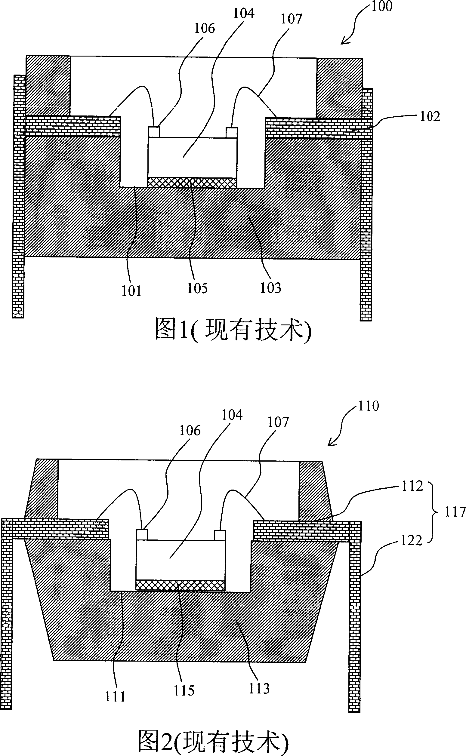
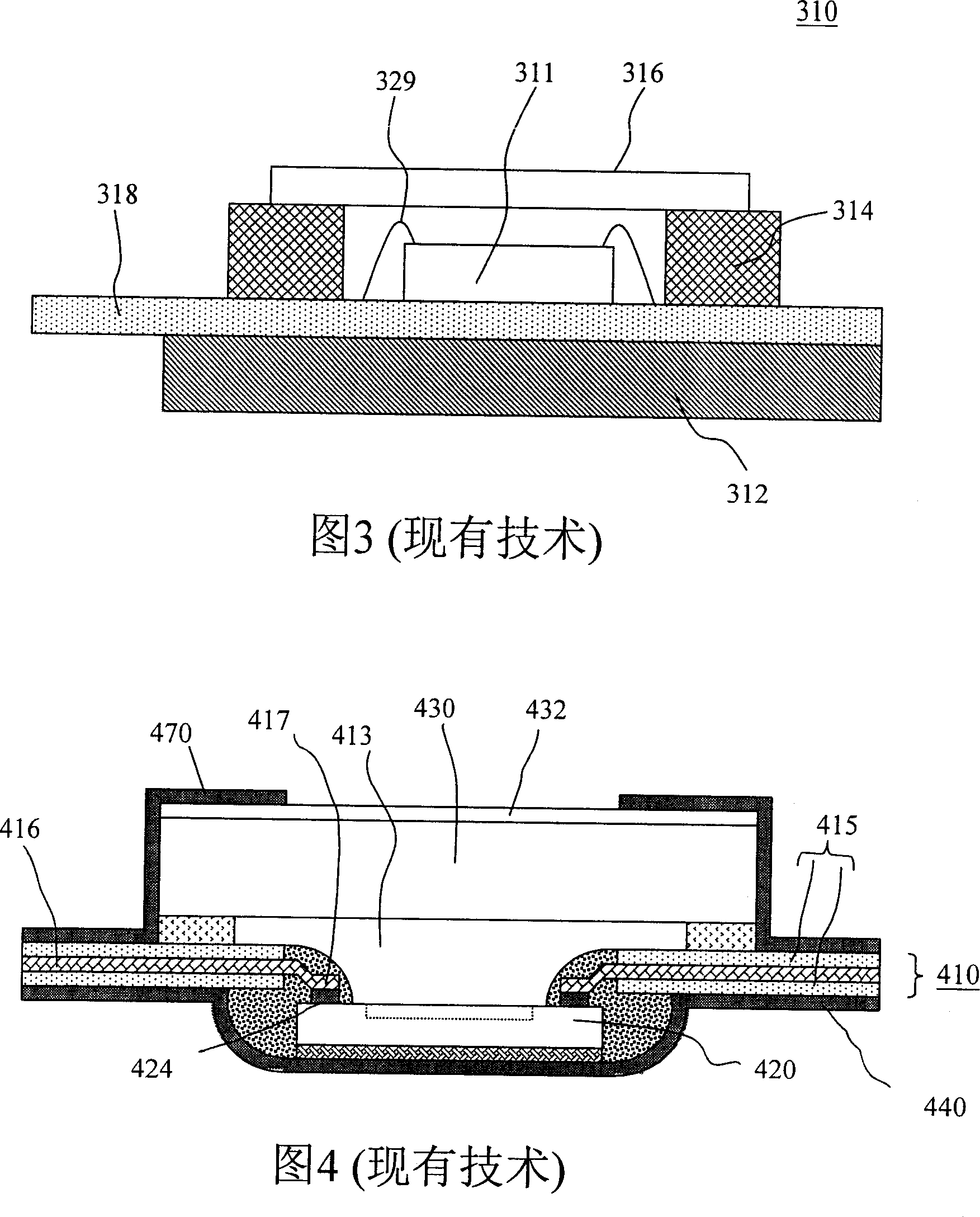
[0095]A photoelectric sensing device according to an embodiment of the present invention includes a photoelectric sensing substrate containing a photoelectric element conversion region and a transparent substrate provided with at least one groove, which are directly bonded to each other by bonding technology, and the concave substrate of the transparent substrate is The groove is an electrode pad corresponding to the photoelectric sensing substrate. In addition, the external electrical connection end of the photoelectric sensing device can be thinned from the upper surface of the transparent substrate to the bottom of the groove, so that the electrode pads inside are exposed or through another connect...


PUM


Abstract

The invention provides a low-noise light-thin photoelectric sensor, comprising a photoelectric sensing base and a transparent base, wherein the photoelectric sensing base comprises a photoelectric converter area, an electrode welding pad which can be used as external electrode connector or an external electrode joint wedge through the photoelectric sensing base, a peripheral circuit surrounding the photoelectric converter area, which is electrically connected with the photoelectric converter area, the electrode welding pad and / or joint wedge on the photoelectric sensing base, or further to be used as the output, input, signal amplification of photoelectric signal, and the decode of pixel address of the photoelectric converter. The transparent base comprises a groove relative to the electrode welding pad, via bonding art to be directly jointed with the transparent base and the base of the photoelectric sensor. The invention has easy assembly, which can support batch production of one integrated chip or at least part of chips of one photoelectric sensor, to simplify the production and reduce production cost. The invention also provides the production method and relative photoelectric sensing modules of photoelectric sensor.

Description

technical field [0001] The invention relates to a photoelectric sensing device, in particular to a low-noise thin photoelectric sensing device. Background technique [0002] In recent years, with the rapid development of the electronic industry, the rapid reduction of the life cycle of various electronic products, and the trend of electronic products towards miniaturization, thinning, and integration of multiple functions, various personal mobile electronic devices are generally equipped with Multimedia photoelectric sensing device modules, other security monitoring systems, medical testing equipment and other thermal imaging systems all have a strong demand for photoelectric sensing devices. [0003] At present, the general photoelectric sensing device is attached to the chip carrier of the ceramic or plastic package, and the electrode pad of the photoelectric sensing device is electrically connected to the internal pins in the package or the circuit board base system by wi...

Claims


Application Information

Patent Timeline
Patent Type & Authority Applications(China)
IPC IPC(8): H01L27/144H01L23/552H01L25/00H01L23/488H01L21/82
CPCH01L2924/0002H01L2224/48091H01L2224/73265H01L24/50H01L2924/01322H01L2924/15787H01L2924/181H01L2224/32225H01L2224/48247H01L2224/50H01L2924/00014H01L2924/00H01L2924/00012
Inventor 曾世宪
Owner 曾世宪
Why Eureka
Try Eureka