High power LED two-dimension light source

A high-power, LED chip technology, applied in the direction of electrical components, circuits, semiconductor devices, etc., can solve the problems of increasing the cost of lamps, large differences in heat conduction paths, and affecting work, so as to improve the level of automated production and improve visual comfort. , The effect of simplifying the manufacturing process

Inactive Publication Date: 2008-01-02
NANJING HANDSON SCI & TECH CORP
View PDF0 Cites 11 Cited by
  • Summary
  • Abstract
  • Description
  • Claims
  • Application Information

AI Technical Summary

Problems solved by technology

There are two major problems in this process: 1. The eccentric positioning will cause the eccentricity of the light spot in the later application of LED products; 2. Improper application of thermal conductive adhesive will cause excessive thermal resistance between the heat sink and the heat dissipation aluminum substrate The heat of the LED cannot be fully dissipated, resulting in an increase in the internal temperature of the LED chip, which seriously affects the light output efficiency and working life of the LED light source
Moreover, when qualified single-chip packaged LED products are finally used, they still cannot be mass-produced by SMT, nor can they be electrically connected by standard connectors; Difficult, it is very cumbersome in structural design and assembly, the heat conduction path of each combined LED is very different, and the heat of some single LEDs cannot be fully dissipated, which will affect the overall work
[0004] At present, the packaging of LED chips above 3 W has encountered great difficulties in heat dissipation. The packaging cost of high-power LED single lamps is relatively high, which will directly increase the cost of lamps and directly affect the promotion and application of high-power LEDs in the lighting field.

Method used


Image

  • High power LED two-dimension light source
  • High power LED two-dimension light source

Examples


Embodiment Construction

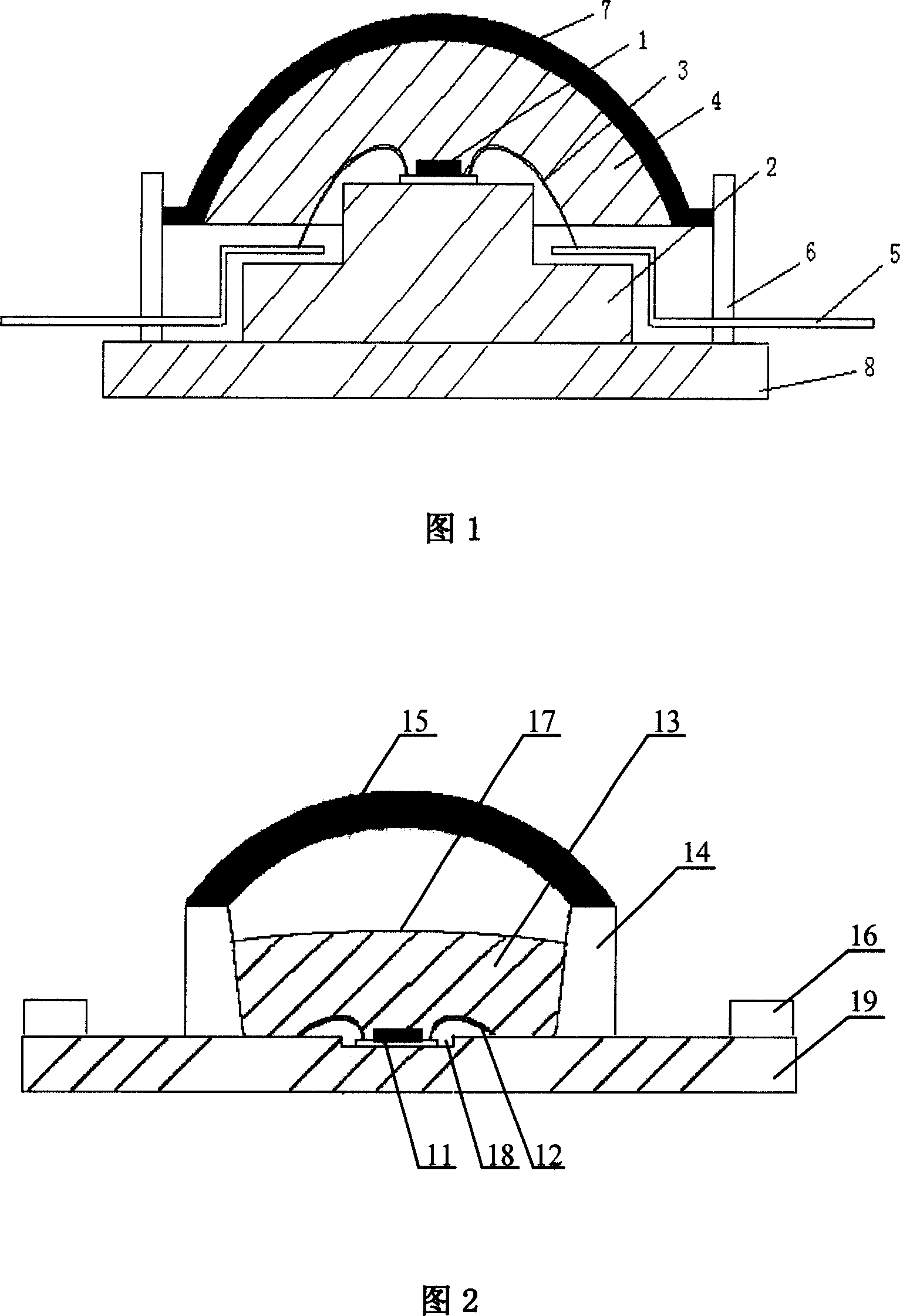
[0023] High-power light-emitting diode (LED) two-dimensional light source, using LED chips directly packaged on metal aluminum-based circuit boards, integrating power chips into one body, forming a low-cost, highly integrated surface light source, with excellent heat dissipation function and uniform luminous effect .

[0024] The structure of the single two-dimensional light source of the present invention is shown in Figure 2, including: a high-power light-emitting diode chip 11, a metal wire 12, a metal aluminum-based circuit board 19 and a bowl-shaped pit 18, a plastic light reflection bowl 14, and a transparent package. Resin 13 and curved surface 17, lens 15 and electrical connection socket 16 molded by process mold.

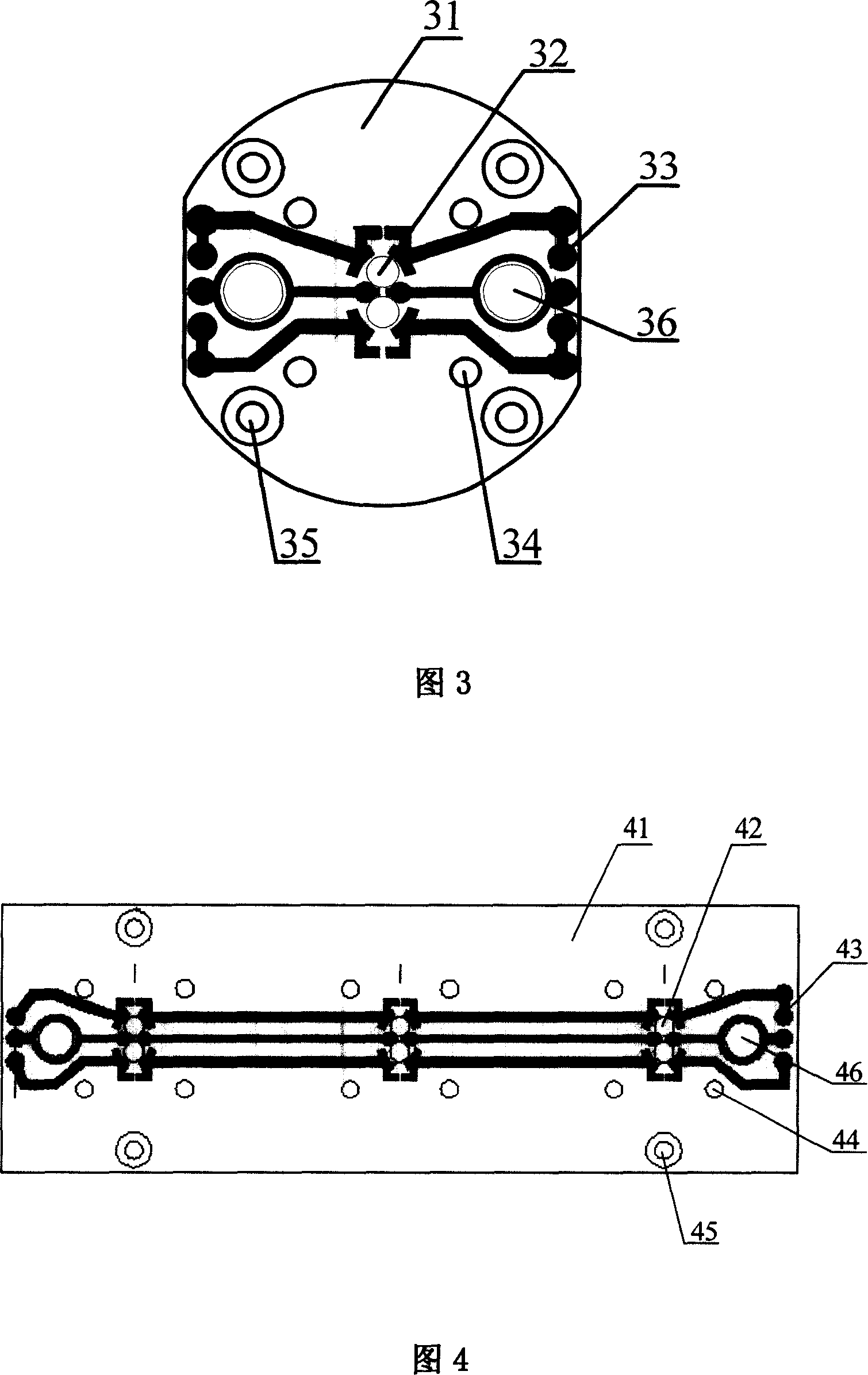
[0025] The metal aluminum-based circuit board of a single two-dimensional light source product is shown in Figure 3. In the figure: aluminum alloy plate 31, bowl-shaped pit 32, plastic light reflection bowl positioning hole 34, standard-spaced pads 33, and ...


PUM


Abstract

The invention provides a high-power LED two-dimension light source, wherein an aluminum-base printed circuit board is directly welded or adhered with a high-power LED chip, the chip welded area is processed with a bowl-shape concave which circumference is furnished and plated with silver to form a light reflective area, the chip is arranged with a light reflective bowl with silver plated at inner surface to be fixed on the aluminum-base circuit board, a chip light outlet is packed with silicon-type transparent resin, in curvature shape, the light reflective bowl is covered with a lens unit, arranged with an electric connecting structure. The invention can be used to produce mono product or multiple beamed product, with standard distance connecting port, surface light source with low cost and high integration, better heat radiation, and uniform lighting effect, which can be used as general semi-conductor lighting source of variable lamps.

Description

technical field [0001] The invention relates to a high-power light-emitting diode (LED) two-dimensional light source, belonging to the technical field of semiconductor lighting. Background technique [0002] In recent years, LED light sources have been increasingly widely used, but the development of single-chip packaged LEDs in the direction of high power has been greatly restricted. The traditional power LED packaging structure is shown in Figure 1, including LED chip 1, heat sink 2, metal wire 3, silica gel 4, bracket 5, plastic seat 6, and lens 7. The bracket 5 is punched out of copper sheet, and the plastic seat 6 with the bracket is included through secondary injection molding; the heat sink 2 is formed by stamping and electroplated, and the heat sink 2 and the plastic seat 6 are embedded, which may be affected by the tolerance of the parts. More defective products with weak assembly are produced; the high-power and large-size LED chip 1 is placed on the heat sink 2, ...

Claims


Application Information

Patent Timeline
Patent Type & Authority Applications(China)
IPC IPC(8): H01L33/00H01L33/48H01L33/56H01L33/58H01L33/60H01L33/64
Inventor 梁秉文刘乃涛张佃环毛家燕
Owner NANJING HANDSON SCI & TECH CORP
Why Eureka
Try Eureka