Phase change memory unit with loop phase change material and its making method

A technology of phase-change memory and phase-change materials, which is applied in the field of micro-nano electronics and can solve problems such as differences in device structure preparation methods

Active Publication Date: 2008-01-09
SHANGHAI INST OF MICROSYSTEM & INFORMATION TECH CHINESE ACAD OF SCI
View PDF1 Cites 22 Cited by
  • Summary
  • Abstract
  • Description
  • Claims
  • Application Information

AI Technical Summary

Problems solved by technology

The present invention has similarities with the idea of ​​using phase-change material nanotubes as storage materials (Chinese invention patent, application number: 200510110783.x), but the biggest difference is that there are great differences in the device structure and its preparation method

Method used


Image

  • Phase change memory unit with loop phase change material and its making method
  • Phase change memory unit with loop phase change material and its making method
  • Phase change memory unit with loop phase change material and its making method

Examples


Embodiment 1

[0043] The preparation process of the phase change memory device unit prepared by utilizing the annular phase change material according to the present invention is as follows:

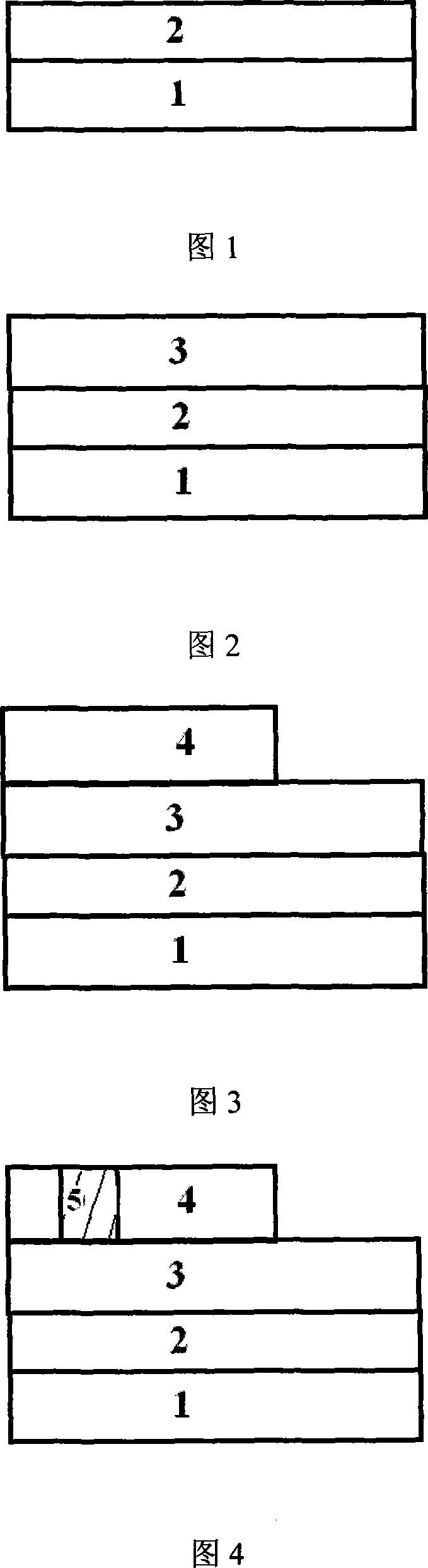
[0044] Step 1: The substrate is a silicon wafer, and a layer of SiO is prepared on the silicon wafer by thermal oxidation 2 The first insulating material layer has a film thickness of 500nm. (figure 1)

[0045] Step 2: On SiO 2 On the first insulating material layer, the lower electrode W thin film is prepared by magnetron sputtering method, and the process parameters are: the background pressure is 1×10 -4 Pa, the Ar gas pressure during sputtering is 0.08Pa, the sputtering power is 400W, the substrate temperature is 25°C, and the film thickness is 100nm. (figure 2)

[0046] Step 3: Prepare SiO on W film by magnetron sputtering 2 For the second insulating film layer, the process parameters are: the background air pressure is 1×10 -4 Pa, the Ar gas pressure during sputtering is 0.12Pa, the sputter...

Embodiment 2

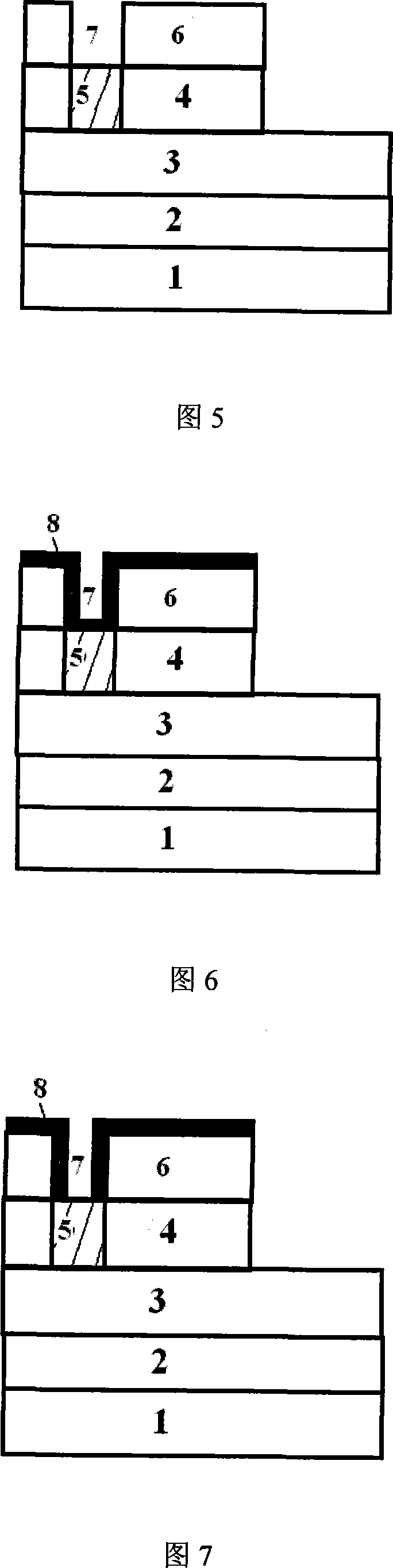
[0056] Change step 5 in embodiment 1 as follows: in SiO 2 Preparation of heat insulating material SiO by PECVD method on heat insulating film and TiN heating electrode material 2 Thin film, the thickness of the film is 200nm; then, conventional photolithography technology is used to expose and etch directly above the heating electrode TiN to prepare a circular hole with a diameter of 200nm, and the heating electrode TiN is exposed in the hole.

[0057] Change step 7 in Example 1 to the following: Reactive ion etching technology is used to etch and remove the phase change material at the bottom of the circular hole to form a ring-shaped phase change material with an outer diameter of 200 nm and a wall thickness of 10 nm.

[0058] The rest of the steps are exactly the same as in Example 1, and a phase change memory device unit whose outer diameter of the annular phase change material is smaller than that of the heating electrode material can be prepared. (Figure 11)

Embodiment 3

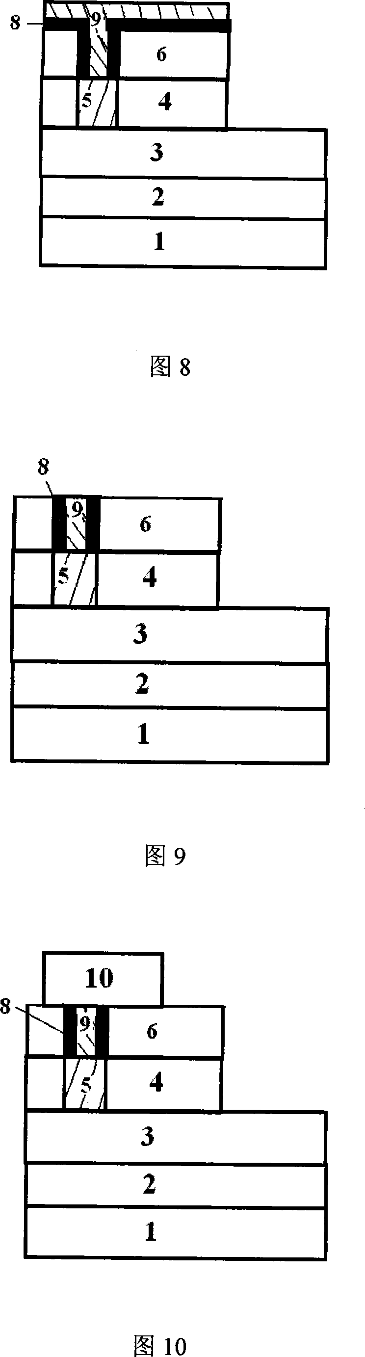
[0060] Change step 5 in embodiment 1 as follows: in SiO 2 Preparation of heat insulating material SiO by PECVD method on heat insulating film and TiN heating electrode material 2 Thin film, the thickness of the film is 200nm; then, conventional photolithography technology is used to expose and etch directly above the heating electrode TiN to prepare a circular hole with a diameter of 350nm, and the heating electrode TiN is exposed in the hole.

[0061] Change step 6 in embodiment 1 as follows: adopt atomic layer deposition technology to prepare Ge in the hole 2 Sb 2 Te 5 Phase change material with a film thickness of 40nm.

[0062] Change step 7 in Example 1 to the following: Reactive ion etching technology is used to etch and remove the phase-change material at the bottom of the circular hole to form a ring-shaped phase-change material with an outer diameter of 350 nm and a wall thickness of 40 nm.

[0063] The rest of the steps are exactly the same as in Example 1, and a...


PUM


Abstract

The invention is concerned with the structure of the phase change memorizer device unit and its making method, with the cycle phase change material made of the heating electrode and the up electrode as the information saving carrier. The cycle phase change material is made of the proper film making technique and the nanometer processing, educed through the up and down electrode and integrated with the switch and the periphery circuit to prepare the nanometer scale phase change memorizer device unit. It is because of the thickness of the wall of the cycle phase change material is controllable within the nanometer scale range, the cross section area of the phase change material can be really small to improves the current density and the thermal efficiency of the phase change material available changing area that reduces the operating current of the phase change memorizer device unit and it's power consumption.

Description

technical field [0001] The invention relates to a non-volatile phase-change memory device unit with ring-shaped phase-change materials and a manufacturing method thereof, belonging to the technical field of micro-nano electronics. Background technique [0002] Phase Change Random Access Memory (PC-RAM, Phase Change-Random Access Memory) technology is based on Ovshinsky in the late 1960s (Phys.Rev.Lett., 21, 1450, 1968) and early 1970s (Appl.Phys.Lett. , 18, 254, 1971) the idea that the phase-change thin film proposed can be applied to the phase-change storage medium is established. The key material of the PC-RAM memory, the phase-change alloy, is characterized in that it can make the material undergo a reversible phase change between amorphous and polycrystalline states when an electric pulse is given to it. It exhibits high resistance in the amorphous state and low resistance in the polycrystalline state, and the variation range can reach several orders of magnitude. Howe...

Claims


Application Information

Patent Timeline
Patent Type & Authority Applications(China)
IPC IPC(8): H01L45/00G11C11/56
Inventor 刘波宋志棠封松林陈宝明
Owner SHANGHAI INST OF MICROSYSTEM & INFORMATION TECH CHINESE ACAD OF SCI
Why Eureka
Try Eureka