
Differential circuit delay unit for high-speed voltage control oscillator

A voltage-controlled oscillator, differential circuit technology, used in electrical components, single output arrangements, automatic control of power, etc.

Inactive Publication Date: 2011-05-11
NAT UNIV OF DEFENSE TECH
View PDF5 Cites 0 Cited by
  • Summary
  • Abstract
  • Description
  • Claims
  • Application Information

AI Technical Summary

Problems solved by technology

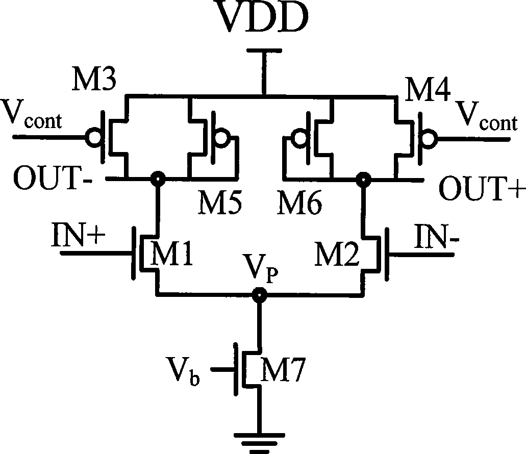
And the delay unit shown in Figure 4 uses MOS tube M3 and M4 are used as load tubes. On the one hand, they are too sensitive to the control voltage; on the other hand, their I-V characteristic curves cannot meet the requirements.
Due to the inherent nonlinear effect of MOS transistors, Figure 4 The I-V curve of the oscillation unit with the structure shown also shows nonlinear characteristics. We always hope that the current can change linearly with the change of voltage, so that the frequency also changes linearly with the change of voltage, but the volt-ampere characteristic curve of a single MOS tube Not linear over a wide range
Then, the linearity of the oscillator formed by connecting the structural stages must be very poor.

Method used


Image

  • Differential circuit delay unit for high-speed voltage control oscillator
  • Differential circuit delay unit for high-speed voltage control oscillator
  • Differential circuit delay unit for high-speed voltage control oscillator

Examples


Embodiment Construction

[0020] The present invention will be described in further detail below in conjunction with the accompanying drawings and specific embodiments.

[0021] Such as Figure 5 As shown, the present invention is used for a differential circuit delay unit of a high-speed voltage-controlled oscillator, which includes a first NMOS transistor M1, a second NMOS transistor M2, a first PMOS transistor M3, a second PMOS transistor M4, a third PMOS transistor M5, The structure of the fourth PMOS transistor M6, the fifth PMOS transistor M7 and the sixth PMOS transistor M8 has no tail current source. Among them, the first NMOS transistor M1 and the second NMOS transistor M2 form a differential pair, the gates of which are respectively connected to the differential inputs IN+ and IN-, the drains of the cross-coupled MOS transistors M3 and M4 are respectively connected to the differential outputs OUT- and OUT+, and the gates The poles are respectively connected to the differential outputs OUT+ a...


PUM


Abstract

The invention discloses a differential circuit delay unit for a high speed voltage controlled oscillator, wherein a first N-channel Metal Oxide Semiconductor (NMOS) tube (M1) and a second NMOS tube (M2) form a differential pair transistor, the grids thereof are respectively connected to differential input IN+ and IN-, the drain electrodes of cross coupled Metal Oxide Semiconductor (MOS) tubes (M3) and (M4) are respectively connected to differential output OUT- and OUT+, and the grids are connected to the differential output OUT+ and OUT-, a third PMOS tube (M5) and a fourth PMOS tube (M6) for delay controlling, are connected to between the differential output nodes OUT-, OUT+ and the power voltageVDD, a control voltage (Vcont) is connected to the grids of the third PMOS tube (M5) and the fourth PMOS tube (M6), a complex load is formed by parallelly connecting the third PMOS tube (M5) and a fifth PMOS tube (M7) which is connected to form the diode, another complex load is formed by parallelly connecting the fourth PMOS tube (M6) and a sixth PMOS tube (M8) which is connected to form the diode, and the fifth PMOS tube (M7) is constantly communicated to the sixth PMOS tube (M8). The invention is the differential circuit delay unit for the high speed voltage controlled oscillator which has simple structure, better process migration performance, and better linearity of the load thereof.

Description

Technical field [0001] The present invention mainly involves the field of pressure -controlled oscillator design in the clock data recovery circuit, which refers to a delay unit for differential circuits for high -speed voltage control oscillator. Background technique [0002] Voltage-Controlled-OSCILLlator (VCO) is one of the key modules in the clock data recovery circuit.In the integrated circuit, the most oscillator structure is the RC ring oscillator and the LC regulating oscillator.The littering performance of the LC tuning oscillator is very good, but because it is difficult to integrate the inductance on the film, it requires the support of the process; and the ring oscillator is widely used in frequency synthesizers, clock generators and data clocks due to simple structure and easy integration.Restore the circuit. [0003] The structure of the ring oscillator is also divided into two structures: single -end and differential structure, which are figure 1 and figure 2 Show....

Claims


Application Information

Patent Timeline
Patent Type & Authority Patents(China)
IPC IPC(8): H03L7/099H03K5/13H03K5/134
Inventor 陈吉华唐世民张民选李少青赵振宇陈怒兴马剑武何小威吴宏欧阳干王建军刘征陈亮王东林王洪海
Owner NAT UNIV OF DEFENSE TECH
Learn More