Control method for epitaxial layer transition zone on re-mixed arsenic underlay

A control method and epitaxial layer technology, applied in semiconductor/solid-state device manufacturing, electrical components, circuits, etc., can solve problems such as difficulty in control, deterioration of forward characteristics, poor controllability of resistivity uniformity, etc. Low efficiency, increased resistivity gradient, good resistivity uniformity

Active Publication Date: 2008-01-23
HEBEI POSHING ELECTRONICS TECH
View PDF0 Cites 7 Cited by
  • Summary
  • Abstract
  • Description
  • Claims
  • Application Information

AI Technical Summary

Problems solved by technology

[0015] First of all, although HCl corrosion at high temperature can polish the substrate and is beneficial to improve the lattice structure, it also has some disadvantages: HCl polishing also produces some by-products, and it also needs to be polished at high temperature. A layer is peeled off the surface of the substrate, so some of these by-products and impurities in the substrate will enter the atmosphere of vapor deposition, thereby affecting the impurity content of the intrinsic epitaxial layer formed in the first step, that is, the transition layer
[0016] Second, there is a greater risk of high-resistance interlayers appearing in the intrinsic epitaxial layer grown in the first step
The As dopant in the heavily doped arsenic substrate will diffuse outward during growth, and it is difficult to control it, which is very likely to cause a high resistance layer in the intrinsic epitaxial layer
[0017] In addition, although this process can greatly improve the uniformity of the epitaxial layer, the test shows that the uniformity of the resistivity can only reach 4%, which cannot be further improved; It is almost impossible to achieve, and the controllability of its resistivity uniformity is extremely poor
[0018] Fourth, this method is effective for preventing vertical self-doping, but not effective for preventing lateral self-doping at the interface
[0020] The above method has a certain effect on controlling the steepness of the epitaxial layer, but for epitaxy with a thinner epitaxial layer, a higher resistivity of the epitaxial layer, or an extremely low resistivity of the substrate, the above methods are difficult to obtain ideal results. And as the thickness of the intrinsic epitaxial layer increases, the forward conduction resistance of the device will also increase, and the forward characteristics will deteriorate; while the silicon-coated base will often affect the roughness and flatness of the back and edge of the epitaxial wafer, resulting in very rough edges. Difficult to pass stepper

Method used


Image

  • Control method for epitaxial layer transition zone on re-mixed arsenic underlay
  • Control method for epitaxial layer transition zone on re-mixed arsenic underlay
  • Control method for epitaxial layer transition zone on re-mixed arsenic underlay

Examples


Embodiment Construction

[0045] Below in conjunction with the specific embodiment of the present invention, the present invention will be described in further detail:

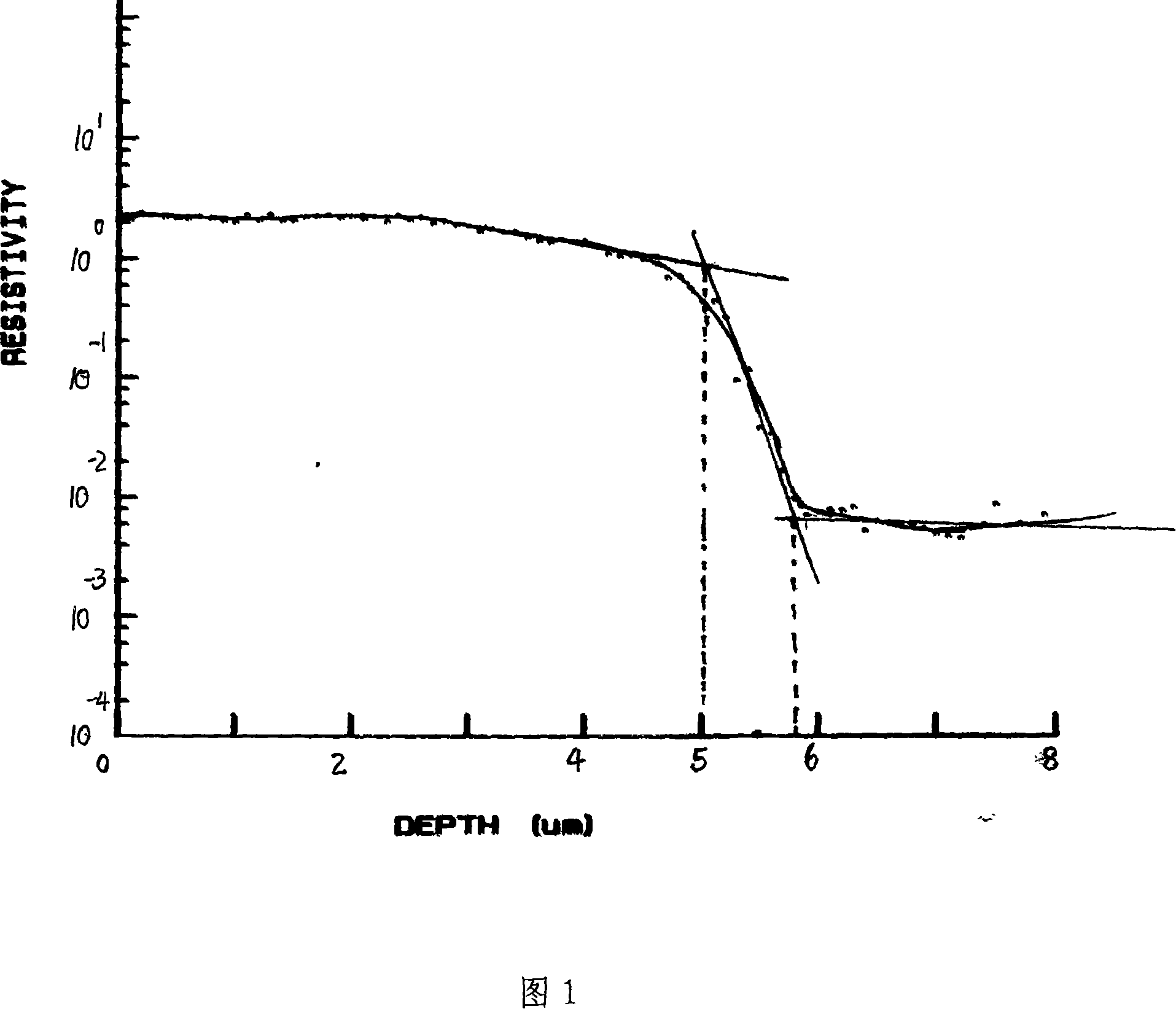
[0046] In the embodiment of the present invention, the measurement and calculation method of the transition zone is as follows: after the sample is ground, the extension resistance analyzer is used to measure the thickness of the epitaxial layer and the longitudinal distribution curve of the resistivity concentration, and then the cross tangent method is used to obtain The thickness of the transition zone, the specific algorithm is shown in Figure 1.

[0047] In this embodiment, the method shown in the present invention is compared with the conventional "two-step epitaxy method". In the two epitaxy methods of the present invention, the specific growth conditions of silicon epitaxy are:

[0048] A main H 2 Flow rate: 100SLM.

[0049] B loading and unloading temperature is 870°C,

[0050] C hydrogen baking temperature is 1160°C,

[...


PUM


Abstract

The invention discloses a control method for an external extension transition section on a heavy doping arsenic underlay, which adopts chemical vapor deposition technology to grow light doping thin silicon extension layer at two times on a n-type heavy doping arsenic silicon underlay. After the growing of a first own extension layer, reduce the temperature to 870 to 930 DEG C. and take it out. During the process, remove the memory effect by putting in a HCI erosion base. After the completion of erosion, place the piece in furnace under the temperature of 870 to 930 DEG C. and then grow the residual extension layer. By checking and comparing the extension layer made with ordinary method and the method in the invention via an extension resistance analyzer, it is proved that the extension layer made of the method in the invention has steepy transition section and resistance of the extension layer has excellent evenness.

Description

technical field [0001] The invention relates to a silicon epitaxial wafer manufacturing technology, in particular to a method for controlling the epitaxial layer transition region on a heavily doped arsenic substrate. Background technique [0002] At present, silicon epitaxial technology on heavily doped arsenic substrate is more and more widely used in the manufacture of electronic devices, and its application scope involves Schottky diodes, triodes, VDMOS, varactor diodes, automotive electronics, IGBTs, etc. In order to improve the yield of dies, manufacturers of electronic components need to strictly control the consistency of silicon epitaxial wafers on heavily arsenic-doped substrates and the transition region of the epitaxial layer. [0003] In the process of chemical vapor deposition, impurities will inevitably appear, and the steepness of impurity distribution in the transition zone between the epitaxial wafer and the substrate will affect the quality and electrical ...

Claims


Application Information

Patent Timeline
Patent Type & Authority Applications(China)
IPC IPC(8): H01L21/205H01L21/30H01L21/302
Inventor 赵丽霞袁肇耿陈秉克薛宏伟
Owner HEBEI POSHING ELECTRONICS TECH
Why Eureka
Try Eureka