
Adhesion preventive silicon capacitance sound transmitter chip and its making method

A condenser microphone, anti-adhesion technology, applied in the direction of electrostatic transducer microphones, sensors, electret electrostatic transducers, etc., can solve the problems of insufficient rigidity, poor frequency response, thin thickness, etc., and achieve guaranteed performance , good performance, avoid the effect of adhesion

Inactive Publication Date: 2008-02-13
INST OF ACOUSTICS CHINESE ACAD OF SCI
View PDF0 Cites 26 Cited by
  • Summary
  • Abstract
  • Description
  • Claims
  • Application Information

AI Technical Summary

Problems solved by technology

However, the back plate in the upper back plate structure is obtained by deposition, the thickness is relatively thin, and the ideal rigidity cannot be achieved, and a "soft back plate" will be formed, which will reduce the sensitivity and frequency response of the microphone.

Method used


Image

  • Adhesion preventive silicon capacitance sound transmitter chip and its making method
  • Adhesion preventive silicon capacitance sound transmitter chip and its making method
  • Adhesion preventive silicon capacitance sound transmitter chip and its making method

Examples


Embodiment 1

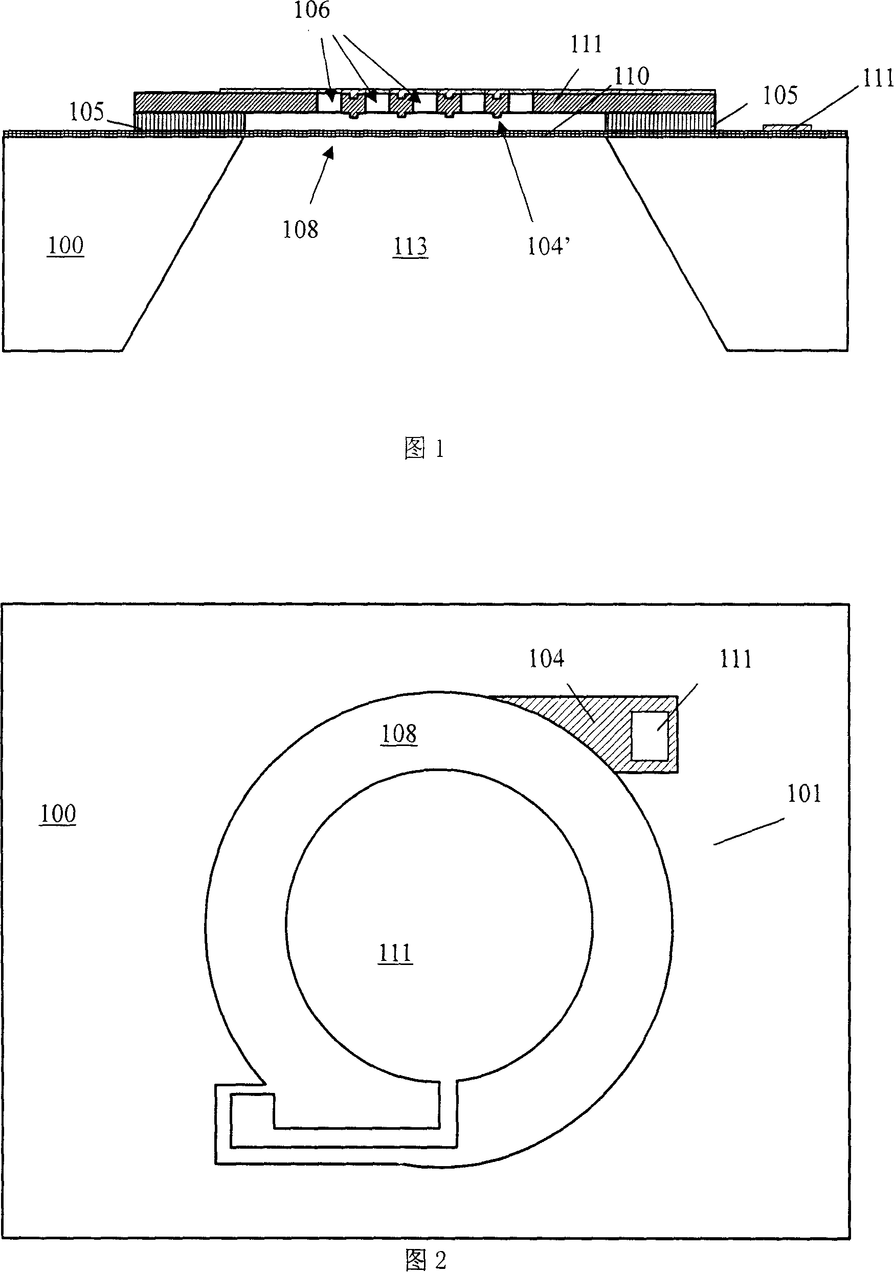
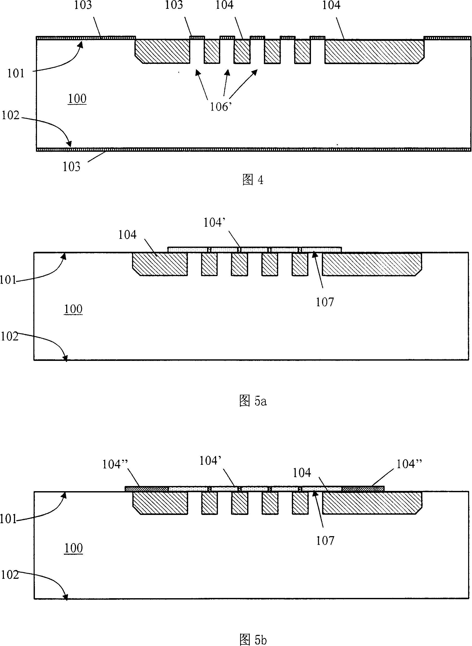
[0041] As shown in Figure 8a, the silicon microcapacitance microphone chip of the present embodiment comprises a silicon substrate 100, on the upper surface 101 of the silicon substrate 100, there is a perforated backplate formed by a doped layer 104, on the perforated backplate Acoustic grid holes 106 are distributed in an array; the upper surface of the doped layer 104 is prepared with an anti-adhesive raised structure 104 ′. There is an annular isolation support layer 105 above the perforated backplane formed by the doped layer 104, and a vibrating membrane 108 is arranged on the isolation supporting layer 105. Electrodes 111 are respectively provided on the surfaces of the vibrating membrane 108 and the doped layer 104, and on the vibrating membrane There is an air gap 110 between 108 and the perforated backplane, and the thickness of the air gap can be between 0.5 microns and 10 microns. The thickness of the isolation support layer 105 is greater than the thickness of the...

Embodiment 2

[0051] As shown in Figure 8a, the silicon microcapacitance microphone chip of the present embodiment comprises a silicon substrate 100, on the upper surface 101 of the silicon substrate 100, there is a perforated backplate formed by a doped layer 104, on the perforated backplate It has acoustic grid holes 106 distributed in an array; the upper surface of the doped layer 104 is prepared with an anti-adhesive raised structure 104', and an annular first isolation support layer 104", the thickness of the first isolation support layer 104" is the same as that of the protrusion Structure 104' is consistent. There is also an annular second isolation support layer 112 above the first isolation support layer 104 ", and the first isolation support layer 104 " and the second isolation support layer 112 constitute the isolation support layer 105; The membrane 108, the surface of the vibrating membrane 108 and the doped layer 104 are respectively provided with electrodes 111, and there is ...

Embodiment 3

[0056] As shown in Figure 8a, the silicon microcapacitance microphone chip of the present embodiment comprises a silicon substrate 100, on the upper surface 101 of the silicon substrate 100, there is a perforated backplate formed by a doped layer 104, on the perforated backplate It has acoustic grid holes 106 distributed in an array; the upper surface of the doped layer 104 is prepared with an anti-adhesive raised structure 104', and the cross-sectional shape of the raised structure 104' can be circular, rectangular, polygonal, etc., and a single raised structure The cross-sectional area of ​​can be between 20 square micrometers and 1000 square micrometers. An exemplary circular protruding structure with a cross-sectional radius of 5 micrometers can be selected, and the thickness of the protruding structure is 0.1 micrometers.

[0057] There is an annular isolation support layer 105 above the perforated backplane formed by the doped layer 104, and a vibrating membrane 108 is ar...


PUM


Abstract

The invention relates to an anti-conglutination silicon micro-condenser microphone chip and a preparation method of the chip including a silicon chip, a perforation backboard, a diaphragm and an electrode. The invention is characterized in that the perforation backboard is arranged on the upward side of the hollow area of the silicon chip. The diaphragm is arranged on the upward side of the perforation backboard and supported by an annular isolating-supporting layer. An air-gap is formed between the diaphragm and the perforation backboard. The upper surface of the perforation backboard is provided with a convex structure. The preparation method comprises the steps of adulterating and preparing the convex structure, depositing a sacrificial layer and a supporting layer, eroding and preparing the diaphragm and the electrode. As the invention has an anti-conglutination and micro-convex structure, the invention avoids conglutinations mainly occurring in a sublimation drying technical process and working process when the sacrificial layer is releasing and greatly improves the qualified rate of apparatus. Simultaneously the convex structure scheme prepared under the lower backboard can prepare to get a thicker backboard which can effectively avoid the problem of soft backboard existed in the preparation of anti-conglutination micro-convex scheme in a former upper backboard structure.

Description

technical field [0001] The invention relates to the field of microelectromechanical systems (MEMS) devices, in particular to an anti-adhesion silicon microcapacitance microphone chip and a preparation method thereof. Background technique [0002] The silicon microcapacitor microphone is a new type of microphone, which usually consists of a silicon chip part and a peripheral circuit part forming a silicon microcapacitor. Among them, the silicon microcapacitor chip is the core of the microphone, which is made on the silicon substrate by using the integrated circuit technology. The silicon microcapacitor chip part is composed of a silicon substrate and a perforated backplane or an acoustic hole backplane, an air gap, an isolation support layer, a vibrating membrane and electrodes. See Micro Electro Mechanical Systems (MEMS), 1998 IEEE 11th International Workshop A HIGH SENSITIVITY POLYSILICONDIAPHRAGM CONDENSER MICROPHONE by P.-C. Hsu, C.H. Mastrangelo, and K.D. Wise, p580-585...

Claims


Application Information

Patent Timeline
Patent Type & Authority Applications(China)
IPC IPC(8): H04R19/01H04R19/04H04R31/00
Inventor 潘昕汪承灏徐联
Owner INST OF ACOUSTICS CHINESE ACAD OF SCI
Learn More