

Fe/Mo nano multilayer film and preparation method thereof
A nano-multi-layer and preparation process technology, which is applied in coating, metal material coating process, ion implantation plating, etc., can solve the problem that the hard metal nano-multi-layer film is not easy to prepare, not suitable for anti-friction applications of machinery and equipment, and has no Rising tribology application research and other issues, to achieve the effect of reliable performance, excellent mechanical properties, and excellent wear resistance
- Summary
- Abstract
- Description
- Claims
- Application Information
AI Technical Summary
Problems solved by technology
Method used
Image

Examples
Embodiment 1
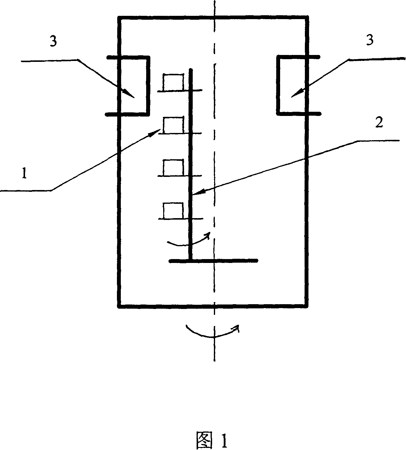
[0032] Mo target and Fe target are respectively placed at the two target source positions;
[0033] The purity of the target material used is: Fe target 90-99.99%; Mo target 90-99.95%;
[0034] The substrate is heated to: 50℃ before coating;
[0035] The working gas is: 99.999% high-purity Ar gas;
[0036] Vacuum degree: 2×10 -4 Pa;
[0037] Working air pressure: 2×10 -2 Pa;
[0038] Negative bias is applied to improve deposition efficiency: 50V;
[0039] Setting voltage: 500V, current 100mA, self-bias 450V, sputtering power 100W;
[0040] When depositing the Mo layer, the residence time of the substrate in front of the Mo target is 9.37 seconds, and the deposition rate is 16 nm / min;
[0041] When depositing the Fe layer, the matrix stays in front of the Fe target for 10 seconds, and the deposition rate is 15 nm / min;
[0042] The thickness of the final Fe / Mo nano-multilayer film bilayer is 5 nm.
Embodiment 2
[0044] Mo target and Fe target are respectively placed at the two target source positions;
[0045] The purity of the target material used is: Fe target 90-99.99%; Mo target 90-99.95%;
[0046] The substrate is heated to: 100℃ before coating;
[0047] The working gas is: 99.999% high-purity Ar gas;
[0048] Vacuum degree: 1×10 -2 Pa;
[0049] Working air pressure: 5×10 -1 Pa;
[0050] Negative bias is applied to improve deposition efficiency: 120V;
[0051] Setting voltage: 800V, current 220mA, self-bias 750V, sputtering power 200W;
[0052] When depositing the Mo layer, the substrate stays in front of the Mo target for 25 seconds, and the deposition rate is 12 nm / min;
[0053] When depositing the Fe layer, the matrix stays in front of the Fe target for 40 seconds, and the deposition rate is 7.5 nm / min;
[0054] The thickness of the final Fe / Mo nano-multilayer film bilayer is 10 nm.
Embodiment 3
[0056] Mo target and Fe target are respectively placed at the two target source positions;
[0057] The purity of the target material used is: Fe target 90-99.99%; Mo target 90-99.95%;
[0058] The substrate is heated to: 150℃ before coating;
[0059] The working gas is: 99.999% high-purity Ar gas;
[0060] Vacuum degree: 2×10 -2 Pa;
[0061] Working air pressure: 2×10 0 Pa;
[0062] Negative bias is applied to improve deposition efficiency: 200V;
[0063] Setting voltage: 1000V, current 400mA, self-bias 950V, sputtering power 300W;
[0064] When depositing the Mo layer, the residence time of the substrate in front of the Mo target is: 100 seconds, and the deposition rate is 6 nm / min;
[0065] When depositing the Fe layer, the matrix stays in front of the Fe target for 100 seconds, and the deposition rate is 6 nm / min;
[0066] The thickness of the final Fe / Mo nano-multilayer film bilayer is 20 nm.
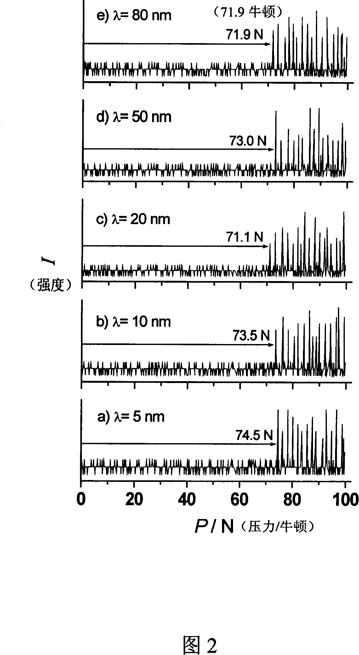
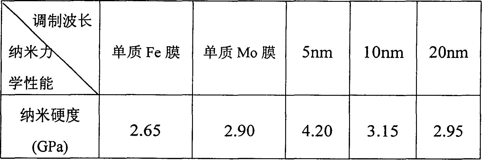
[0067] After testing, the mechanical property parameters of the Fe / Mo...
PUM
| Property | Measurement | Unit |
|---|---|---|
| thickness | aaaaa | aaaaa |
| thickness | aaaaa | aaaaa |
| hardness | aaaaa | aaaaa |
Abstract
Description
Claims
Application Information