

Printed wiring board and its manufacture
A technology for printed circuit boards and manufacturing methods, which is applied in multilayer circuit manufacturing, secondary processing of printed circuits, and assembly of printed circuits with electrical components. Poor bonding performance, small contact area between wiring and solder mask, etc., to eliminate the difference in wettability, excellent bonding performance, and prevent wiring damage
- Summary
- Abstract
- Description
- Claims
- Application Information
AI Technical Summary
Problems solved by technology
Method used
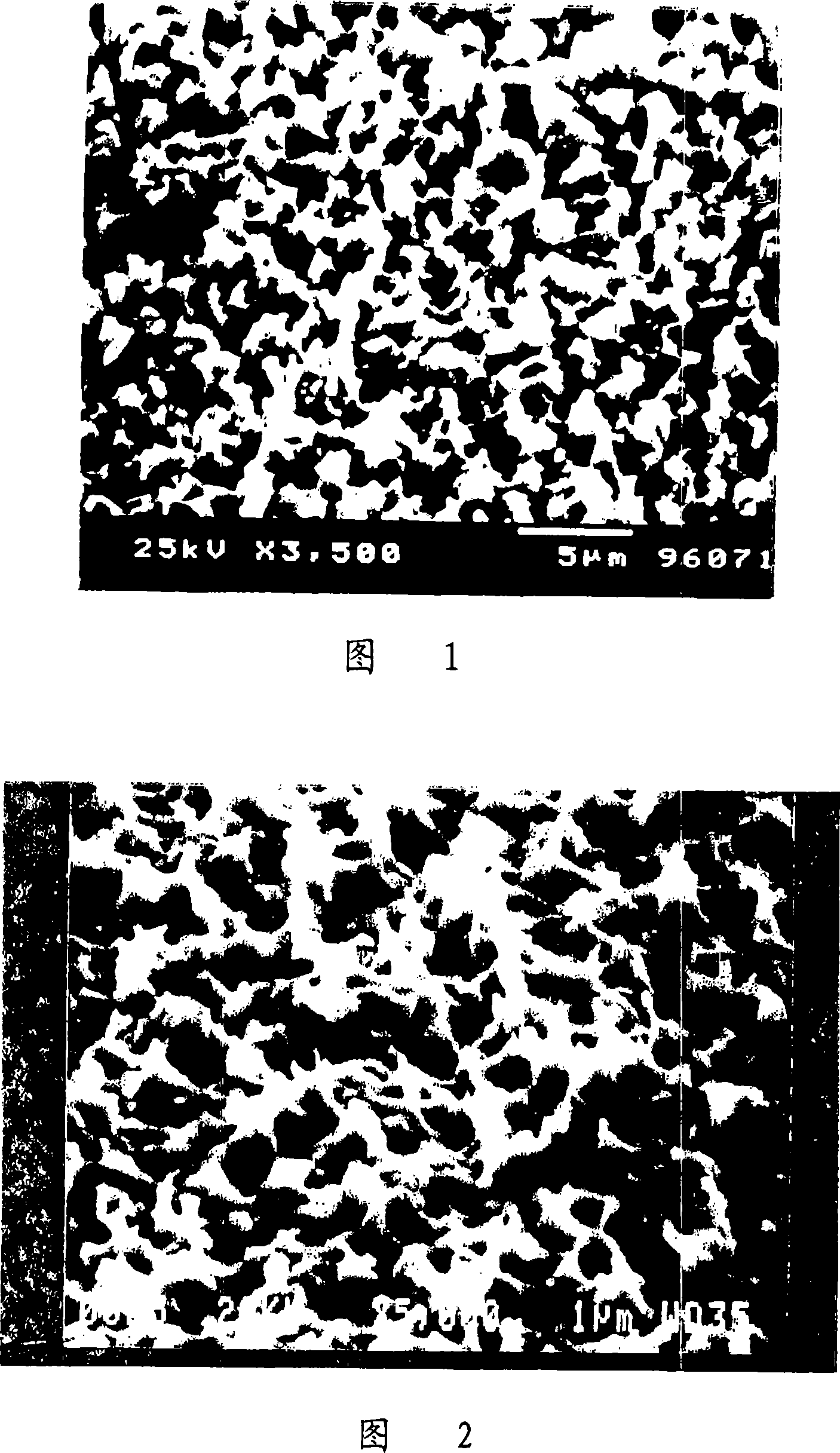
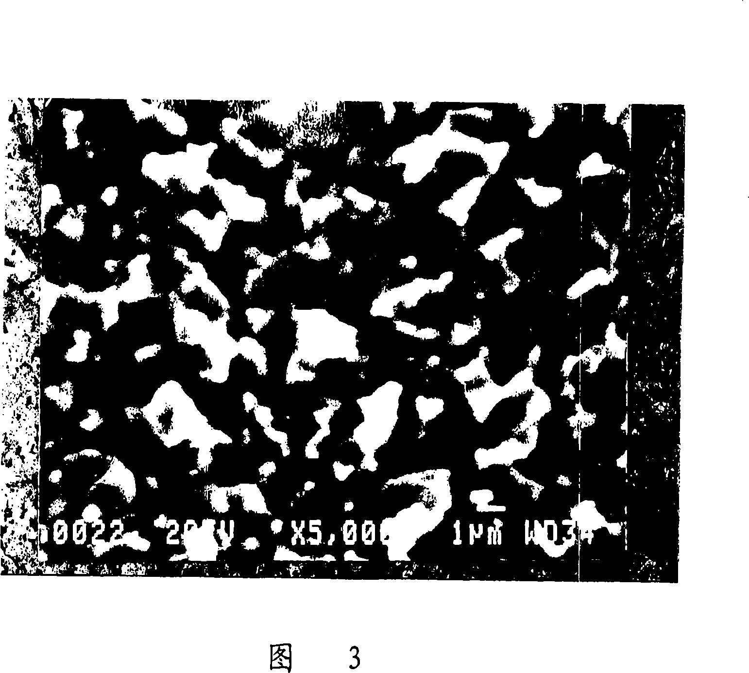
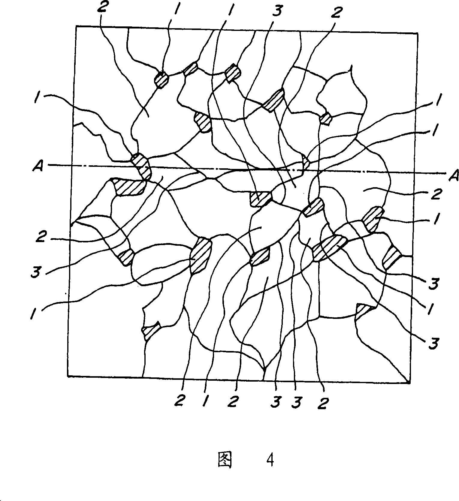
Image

Examples
Embodiment 1
[0205] Preparation of Starting Compositions for Electroless Plating Adhesives
[0206] (Adhesive for upper layer)
[0207] [Resin composition A]
[0208] 35 parts by weight of a resin solution formed by dissolving 25% cresol novolak type epoxy resin with a molecular weight of 2500, manufactured by Nippon Kayaku Co., Ltd. in a concentration of 80 wt% DMDG, Toa Gosei.Co., Ltd. 3.15 parts by weight of a photosensitive monomer manufactured under the trade name Aronix M315, 0.5 parts by weight of an antifoaming agent manufactured by Sannopuco Co., Ltd. under the name S-65, and 3.6 parts by weight of NMP were mixed under stirring to prepare the resin Composition A.
[0209] [Resin composition B]
[0210] 12 parts by weight of polyethersulfone (PES), manufactured by Sanyo Kasei Co., Ltd under the trade name Polymerpole, 7.2 parts by weight of epoxy resin particles with an average particle size of 1.0 μm, and the same resin with an average particle size of 0.5 μm 3.09 parts by...
Embodiment 2
[0272] FIG. 33 is a cross-sectional view of the printed circuit board 44 . The manufacturing steps of this example are basically the same as those in Example 1, except that the rough surface of the wiring surface layer for the pad is covered with a metal layer 51, as shown in FIGS. 9 to 12 in step (17). The metal can be nickel, and the metal film layer is formed by electroless plating. The nickel layer thus formed had a thickness of 0.04 µm.
[0273] In this example, on the solder resist layer 38, pass through the nickel-plated layer 52 on the nickel layer 51, and on the opening part of the gold-plated layer 53 on it, form a solder bump (solder body) 54, as steps (18) to (21) shown in Figure 33.
Embodiment 3
[0275] This example is basically the same as Example 2, except that the tin layer of displacement plating is used instead of the nickel layer of electroless plating as the metal layer on the wiring rough surface for covering pads. The tin layer is 0.03 μm thick.
PUM
| Property | Measurement | Unit |
|---|---|---|
| thickness | aaaaa | aaaaa |
| thickness | aaaaa | aaaaa |
| viscosity | aaaaa | aaaaa |
Abstract
Description
Claims
Application Information