Flash memory device and manufacturing method thereof

A device and control gate technology, applied in the field of flash memory devices and its manufacturing, can solve the problems of low programming and erasing operation speed, difficulty in obtaining wide storage window, SONOS limitations, etc.

Inactive Publication Date: 2008-02-27
DONGBU HITEK CO LTD
View PDF1 Cites 6 Cited by
  • Summary
  • Abstract
  • Description
  • Claims
  • Application Information

AI Technical Summary

Problems solved by technology

However, when a SONOS device is used in a flash memory device, the SONOS has limitations due to the following problems
[0008] Due to the low density of well sites remaining in the silicon nitride film, the programming and erasing operation speed is low, thus, it is difficult to obtain a wide memory window
Due to the narrow energy level of the well site remaining in the silicon nitride thin film, the

Method used


Image

  • Flash memory device and manufacturing method thereof
  • Flash memory device and manufacturing method thereof
  • Flash memory device and manufacturing method thereof

Examples


Embodiment Construction

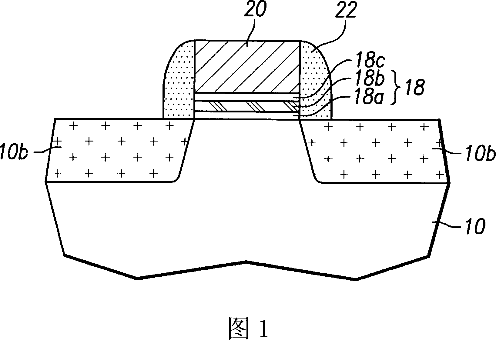
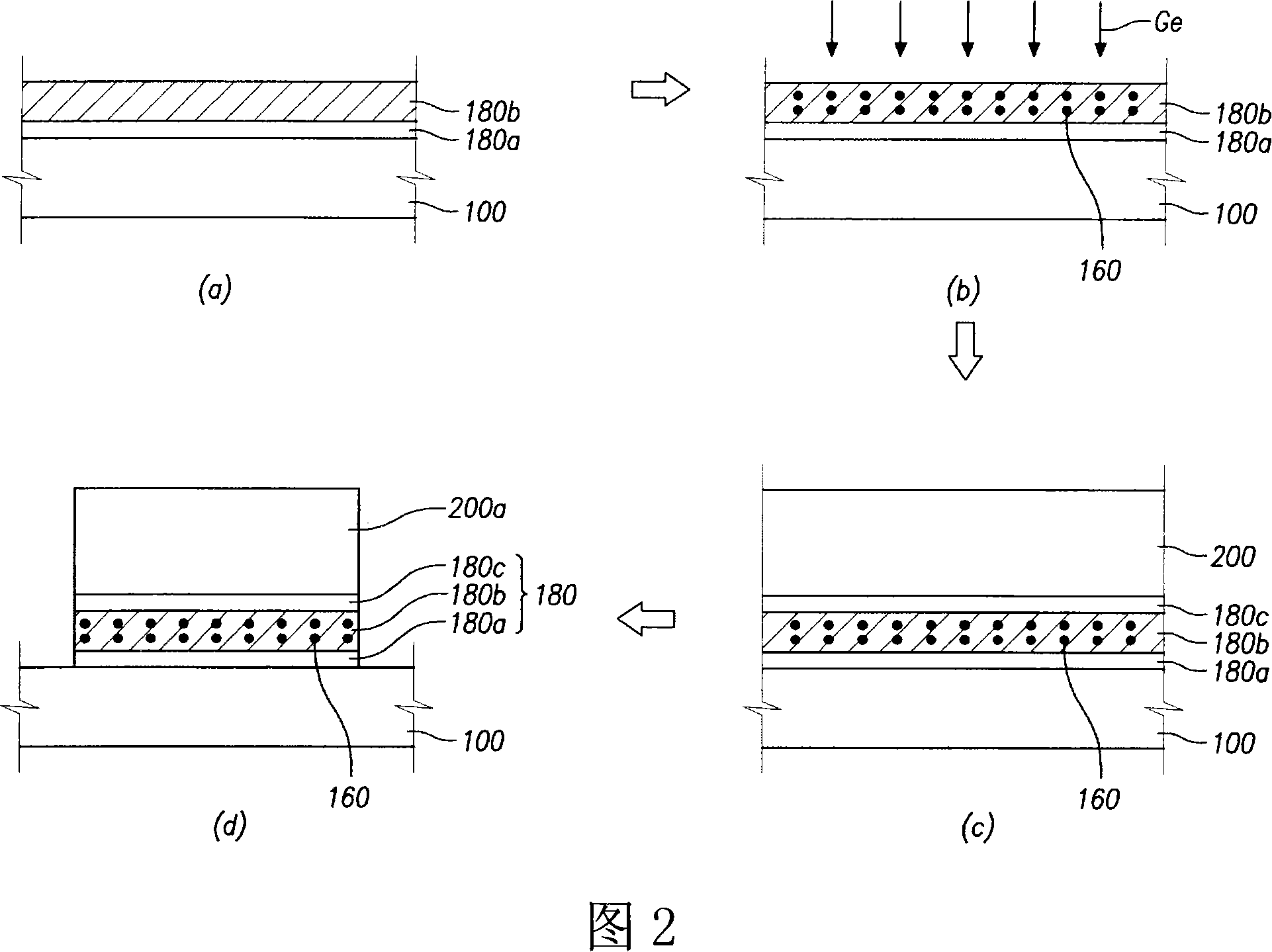
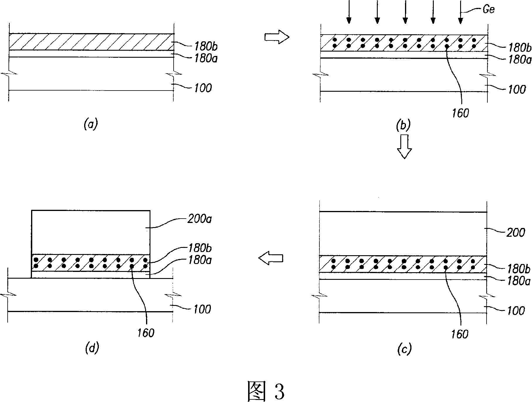
[0016] FIG. 2 is a cross-sectional view illustrating a method of fabricating a flash memory device according to embodiments described herein.

[0017] First, as shown in (a) of FIG. 2, a silicon oxide film is formed on a silicon semiconductor substrate 100 having a thickness between about 15 Ȧ and about 40 Ȧ, wherein the silicon oxide film is used as a tunnel oxide film 180a. In this case, the silicon oxide film 180a may be a thermally oxidized film formed by oxidizing the substrate 100, or may be deposited by chemical vapor deposition (CVD) or physical vapor deposition (PVD). After forming the tunnel oxide film 180a, a silicon nitride film 180b is formed by CVD or PVD, wherein the silicon nitride film 180b is formed to a thickness between about 50 Ȧ and about 250 Ȧ. The silicon nitride film 180b functions as a charge storage layer in which electrons or holes are trapped or de-trapped in the operation of the flash memory device. Generally, the tunnel oxide film 180a, the sili...


PUM

PropertyMeasurementUnit
Sizeaaaaaaaaaa

Abstract

The invention relates to a flash memory device and a manufacturing method thereof, comprising a source diffusion zone and a drain diffusion zone in an active region of a silicon semiconductor substrate for fixing the distance, a multilayer charge storage layer on the substrate, and a control gate formed on the charge storage layer, wherein, the charge storage layer comprises a tunnel oxide film formed on the silicon semiconductor substrate, a silicon nitride film formed on the tunnel oxide film including a plurality of small crystal by injecting the 14 group elements into the silicon nitride film. The flash memory device maintains a good programme and erasure operation of the SONOS device and improves the trap density and memory window. Owing to the energy barrier difference between the small crystal and the silicon nitride, the electron or cavity captured by the small crystal of the deep trap are not easy to escape so as to improve the data memory performance of the device.

Description

[0001] This application claims the benefit of Korean Patent Application No. 10-2006-0080096 filed on Aug. 23, 2006, the entire contents of which are incorporated herein by reference. technical field [0002] The present invention relates to a semiconductor device, in particular to a flash memory device and a manufacturing method thereof. Background technique [0003] Generally, a flash memory is a type of PROM (Programmable Read Only Memory) that enables data to be rewritable electrically. The flash memory performs a program input method of EPROM (Erasable PROM) and a program erasure method of EEPROM (Electrically Erasable PROM). EPROMs typically have a small cell area because each memory cell is composed of one transistor. However, EPROM has a disadvantage in that data can be erased by UV rays. In contrast, in the case of EEPROM, it is only possible to electrically erase data; but EEPROM has a disadvantage of a large cell area because a memory cell is composed of two tran...

Claims


Application Information

Patent Timeline
IPC IPC(8): H01L27/115H01L29/792H01L29/51H01L21/8247H01L21/336H01L21/28
CPCH01L29/7881H01L21/28282H01L29/42348H01L29/792H01L21/28273H01L29/42332H01L29/40114H01L29/40117H01L21/26513
Inventor 郑真孝
Owner DONGBU HITEK CO LTD
Why Eureka
Try Eureka