Double electric capacity metal oxide semiconductor silicon based high speed high modulate efficiency electro optic modulator

An electro-optic modulator and high modulation technology, applied in the direction of optical waveguide and light guide, can solve the problems of increased silicon refractive index, device temperature rise, device failure, etc.

Inactive Publication Date: 2008-03-05
INST OF SEMICONDUCTORS - CHINESE ACAD OF SCI
View PDF0 Cites 12 Cited by
  • Summary
  • Abstract
  • Description
  • Claims
  • Application Information

AI Technical Summary

Problems solved by technology

The silicon-based modulator working under high current will cause the temperature of the device to rise, and the rise of temperature will cause the increase of the refractive index of silicon due to the thermo-optic effect, which offsets the decrease of the refractive index caused by the plasmonic dispersion effect, thus possibly disable the device

Method used


Image

  • Double electric capacity metal oxide semiconductor silicon based high speed high modulate efficiency electro optic modulator
  • Double electric capacity metal oxide semiconductor silicon based high speed high modulate efficiency electro optic modulator
  • Double electric capacity metal oxide semiconductor silicon based high speed high modulate efficiency electro optic modulator

Examples


Embodiment Construction

[0025] Specific embodiments of the present invention will be described below in conjunction with the accompanying drawings.

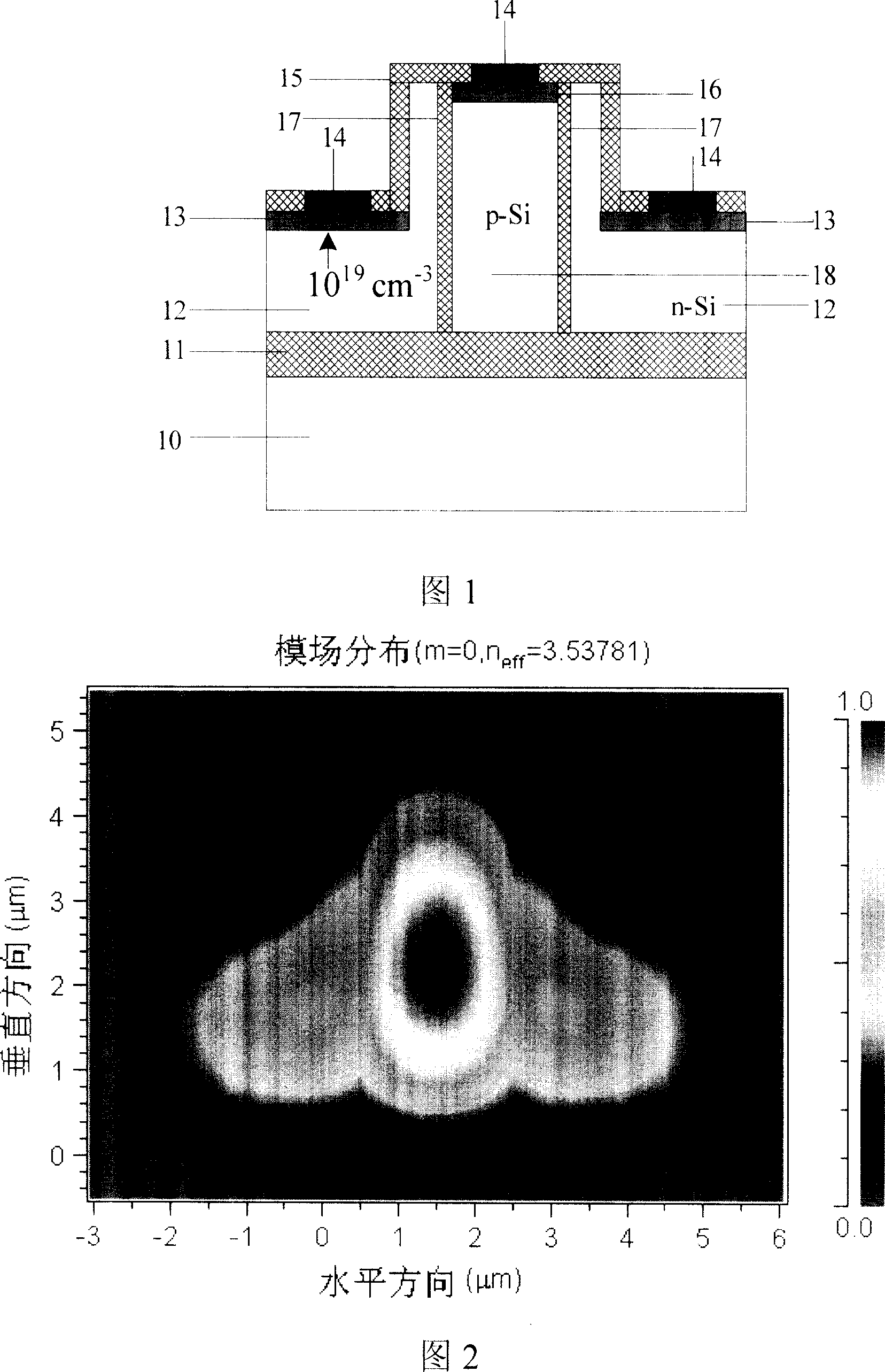
[0026] Please refer to Fig. 1. Fig. 1 shows a cross-sectional view of a MOS modulator with a double vertical gate oxide layer structure. A dual-capacitance MOS silicon-based high-speed high-modulation efficiency electro-optic modulator of the present invention includes:

[0027] a substrate 10;

[0028] A silicon dioxide buried layer 11, the silicon dioxide buried layer 11 is located on the substrate 10;

[0029] A p-type single crystal silicon layer 18, the p-type single crystal silicon layer 18 is single crystal silicon on the substrate, and gate oxide layers 17 are formed on both sides of the p-type single crystal silicon layer 18;

[0030] A p+ injection layer 16, the p+ injection layer 16 is made on the top of the p-type single crystal silicon layer 18;

[0031] An n-type single crystal silicon layer 12, the n type single crystal silicon layer 12...


PUM


Abstract

The invention comprises: a substrate; a silica buried layer formed on the substrate; a p type monocrystalline silicon layer is uses as the monocrystalline silicon on the substrate; forming a grid oxide layer on both sides of the p type monocrystalline silicon layer; a p+ injection layer is formed on the p type monocrystalline silicon layer; a n type monocrystalline silicon layer is formed on the silica buried layer and the both sides of the grid oxide layer, and said n type monocrystalline silicon layer and p type monocrystalline silicon layer are combined together to form a ridge waveguide structure; a n+ injection layer formed on the planes at both sides of the n type monocrystalline silicon ridge waveguide structure; a metal contact layer is formed on middle portion of the p+ injection layer in order to form the positive and negative electrode of the modulator; a oxide layer formed on the surfaces of the n type monocrystalline silicon layer and p type monocrystalline silicon as a protective layer.

Description

technical field [0001] The invention relates to an electro-optic modulator, in particular to a double-capacitance metal oxide semiconductor (MOS) silicon-based high-speed high-modulation-efficiency electro-optic modulator compatible with modern large-scale integrated circuit technology. Background technique [0002] The integration level of integrated circuits is rapidly advancing at a speed of doubling every two years according to Moore's Law, and the simultaneous reduction in the size of transistors and interconnection lines makes the integration level of chips higher and lower, and the cost is getting lower and lower. Although the delay of a single transistor is getting smaller and smaller as the level of integration increases, the delay of interconnect lines is getting bigger and bigger. This is because the reduction in the size of the interconnection wires increases the resistance of the interconnection wires. Although the use of copper interconnections instead of the p...

Claims


Application Information

Patent Timeline
Patent Type & Authority Applications(China)
IPC IPC(8): G02B6/12
Inventor 陈弘达黄北举刘海军顾明
Owner INST OF SEMICONDUCTORS - CHINESE ACAD OF SCI
Why Eureka
Try Eureka