Forming method of metal oxide semiconductor device grids structure

A technology of oxide semiconductor and gate structure, which is applied in the direction of semiconductor devices, semiconductor/solid-state device manufacturing, electrical components, etc., can solve the problems of reduced production efficiency, increased etching difficulty, substrate surface contamination, etc., to achieve easy removal, Easy to remove, good contour effect

Inactive Publication Date: 2008-03-12
SEMICON MFG INT (SHANGHAI) CORP +1
View PDF1 Cites 12 Cited by
  • Summary
  • Abstract
  • Description
  • Claims
  • Application Information

AI Technical Summary

Problems solved by technology

Although this method can obtain a gate with a better profile, the carbon-containing adhesion layer 130 is likely to pollute the substrate surface during the etching process and form dielectric layer

Method used


Image

  • Forming method of metal oxide semiconductor device grids structure
  • Forming method of metal oxide semiconductor device grids structure
  • Forming method of metal oxide semiconductor device grids structure

Examples


Embodiment Construction

[0033] In order to make the above objects, features and advantages of the present invention more comprehensible, specific implementations of the present invention will be described in detail below in conjunction with the accompanying drawings.

[0034] In the following description, numerous specific details are set forth in order to provide a thorough understanding of the present invention. However, the present invention can be implemented in many ways other than those described here, and those skilled in the art can make similar extensions without departing from the connotation of the present invention. Accordingly, the invention is not limited to the specific implementations disclosed below.

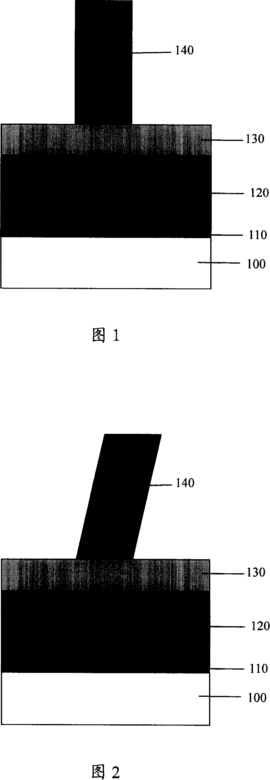
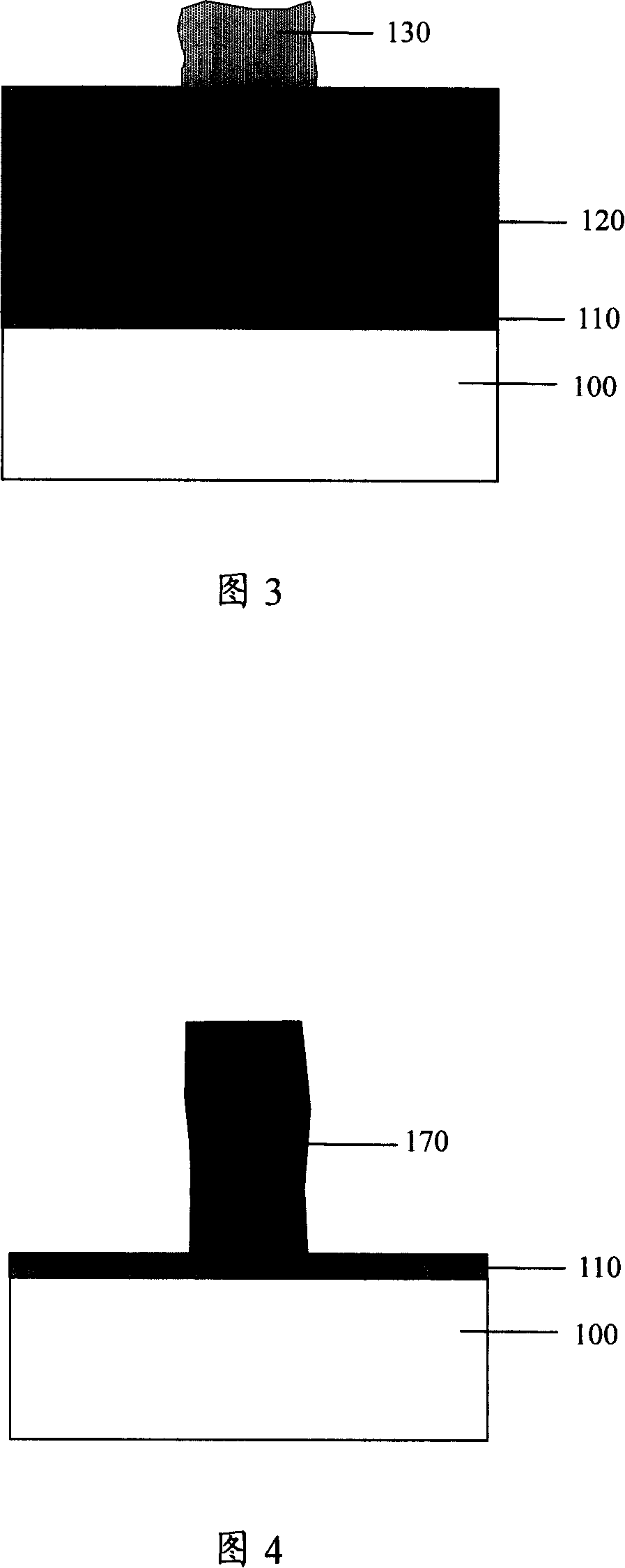
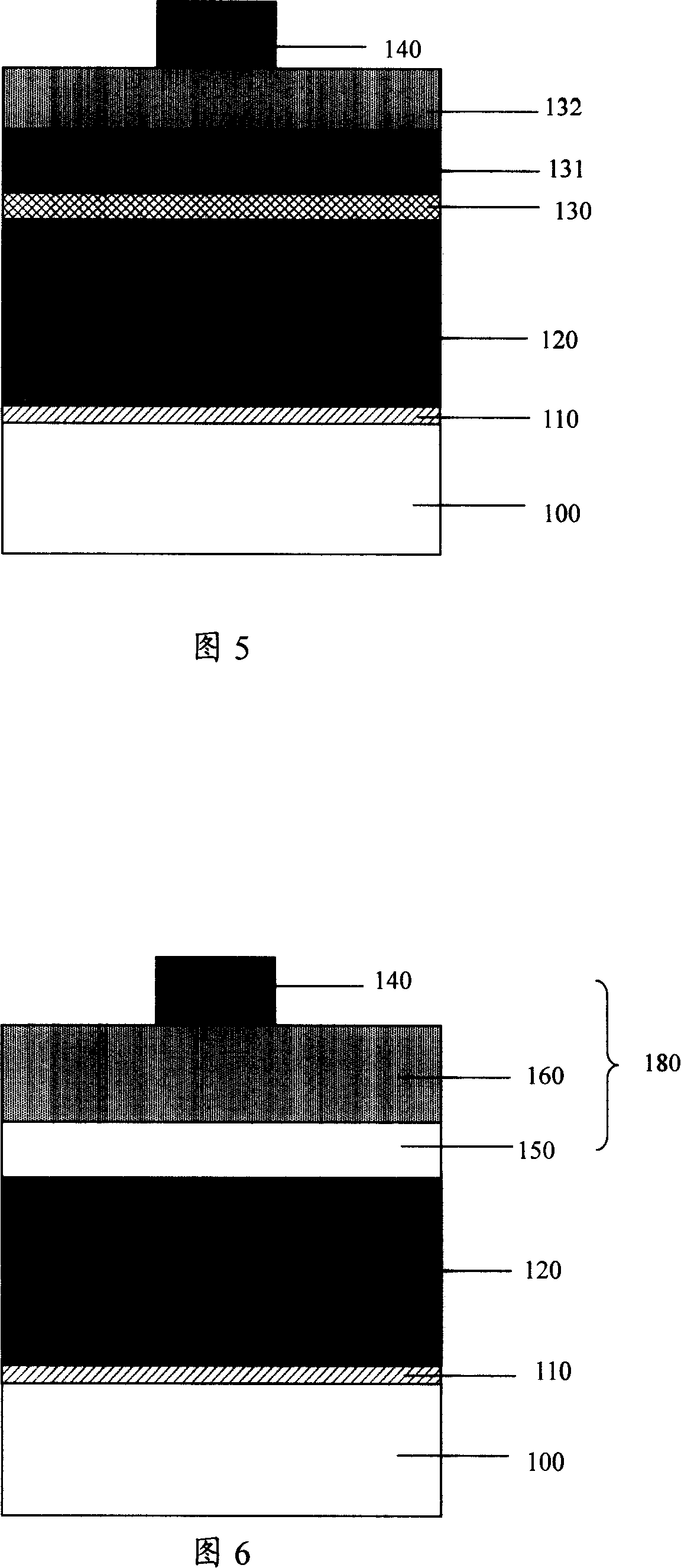
[0035] The method for forming the gate structure of metal oxide semiconductor devices provided by the present invention is particularly suitable for the manufacture of gates of semiconductor devices with a feature size of 65nm or below. The semiconductor device is not only a MOS trans...


PUM

PropertyMeasurementUnit
Thicknessaaaaaaaaaa
Thicknessaaaaaaaaaa
Thicknessaaaaaaaaaa

Abstract

The invention provides a grid structure forming method for semiconductor device of metal oxide, which comprises forming dielectric layer on the semiconductor underlay; forming polycrystalline silicon layer on the said dielectric layer; forming stack layer and positioning the grid location on the said polycrystalline silicon layer; etching the said polycrystalline silicon layer for the mask layer by the said stack layer to form grid; The invention can produce grid with good shape without forming the hard mask layer, which is especially applicable to grid making with characteristic dimension of line width under 65nm.

Description

technical field [0001] The invention relates to the technical field of semiconductor manufacturing, in particular to a method for forming a gate structure of a metal oxide semiconductor device. Background technique [0002] Polysilicon is the preferred material for manufacturing gates, which has special heat resistance and high etching pattern accuracy. The manufacturing method of the gate first needs to form a layer of gate silicon oxide on the semiconductor substrate, then deposit a polysilicon layer on the gate oxide layer, and then coat a fluid bottom anti-reflection layer (BARC) and photoresist. After patterning the photoresist layer, etching the polysilicon layer to form a gate. 1 to 4 are schematic cross-sectional views illustrating a conventional gate manufacturing method. As shown in FIG. 1 , a gate oxide layer 110 is grown on a substrate 100 , a polysilicon layer 120 is deposited on the gate oxide layer 110 , and then the polysilicon layer is etched to form a gat...

Claims


Application Information

Patent Timeline
IPC IPC(8): H01L21/28H01L21/336
Inventor 张海洋刘乒马擎天陈海华
Owner SEMICON MFG INT (SHANGHAI) CORP
Why Eureka
Try Eureka