Through-hole etching method

A technology of through-hole etching and etching gas, which is applied in the directions of optics, instruments, and opto-mechanical equipment. Stability, effect of improving density

Active Publication Date: 2008-03-12
SEMICON MFG INT (SHANGHAI) CORP +1
View PDF1 Cites 13 Cited by
  • Summary
  • Abstract
  • Description
  • Claims
  • Application Information

AI Technical Summary

Problems solved by technology

Usually, the photoresist layer is soft and vulnerable to damage during the etching process, which is equivalent to changing the design size and causing via hole etching stripe defects. For deep sub-micron process nodes, this via etching stripe Defects can easily cause interconnections between vias, which in turn cause short circuits between metal lines and cause device performance failure

Method used


Image

  • Through-hole etching method
  • Through-hole etching method
  • Through-hole etching method

Examples


no. 1 example

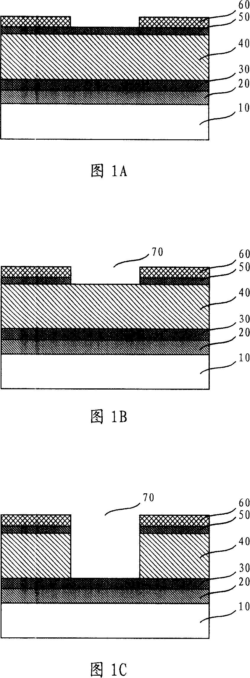
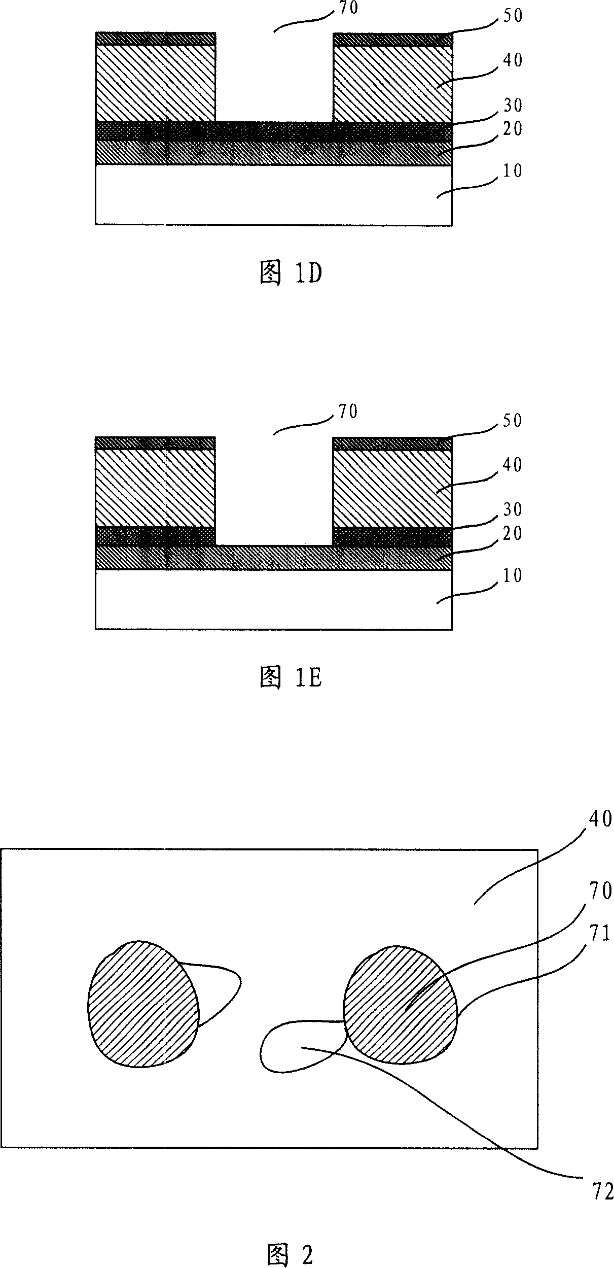
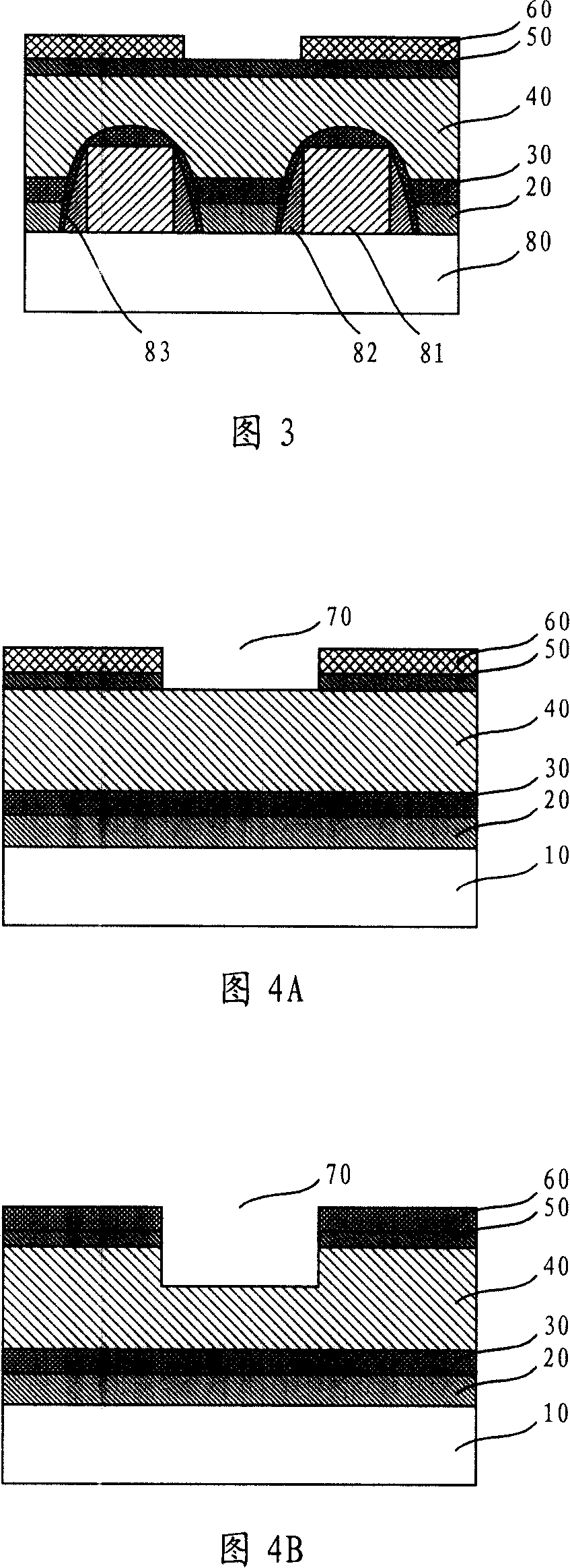
[0025] 4A to 4E are schematic diagrams illustrating a through-hole etching method of the first embodiment of the method of the present invention. As the first embodiment of the present invention, the specific steps of applying the method of the present invention to etch the through-hole of the inter-metal dielectric layer are as follows:

[0026] First, as shown in FIG. 4A , a via hole etching structure is formed on the surface of the underlying metal 10 , and the anti-reflection coating 50 is etched.

[0027] The etched structure of the through hole 70 includes an adhesive layer 20 , an etch stop layer 30 , a dielectric layer 40 , an antireflection coating 50 and a patterned photoresist layer 60 deposited in sequence. The bonding layer 20 is a transition layer that enhances the connection effect between the semiconductor substrate and the connection material in the through hole; the etching stop layer 30 is an etching stop layer; the dielectric layer 40 includes an insulating ...


PUM

PropertyMeasurementUnit
thicknessaaaaaaaaaa
thicknessaaaaaaaaaa
heightaaaaaaaaaa

Abstract

A pylome etching method is provided, which comprises: forming pylome etching structure, which includes adhesive coating sedimentary in sequence, etch stop layer, dielectric layer and patterned photoresist layer; etching antireflective coating; etching dielectric layer; eliminating photoresist layer; etching the etch stop layer; The etching process of the said dielectric layer includes the first etching process and the second etching process etched respectively by the first etching gas and the second etching gas. The method provided in the invention can improve the tightness of the photoresist layer to effectively control the appearance of the etching pylome, further adjust the both transverse and lognitudinal etching selection ratio and precisely control the shape of the etching pylome to avoid damage to sidewall of the gird and guarantee the normal operation of the device.

Description

technical field [0001] The invention relates to the technical field of semiconductor manufacturing, in particular to a through hole etching method. Background technique [0002] VLSI (Very Large Scale Integrated Circuit, VLSI) usually requires more than one metal layer to provide sufficient interconnection capacity. The through holes filled with conductive materials are realized, and in order to ensure the stability of the device, there is no electrical connection between the through holes, which makes it very important to strictly control the through hole etching process. With the increasing density of devices and complexity of processes, higher requirements are placed on the via etching process. [0003] 1A to 1E are schematic diagrams illustrating methods for etching through holes in the prior art. In the prior art, etching through holes refers to etching the etching structure of the through holes to obtain the interconnection between multilayer metals and the active par...

Claims


Application Information

Patent Timeline
Patent Type & Authority Applications(China)
IPC IPC(8): H01L21/311G03F7/00
Inventor 韩秋华
Owner SEMICON MFG INT (SHANGHAI) CORP
Why Eureka
Try Eureka