TFT matrix structure and making method thereof

A technology of matrix structure and manufacturing method, which is applied in semiconductor/solid-state device manufacturing, optics, instruments, etc., can solve problems affecting channel width-to-length ratio, complex multi-step etching process, and change of TFT electrical characteristics, so as to reduce short circuit occurrence, saving chemical solution, and reducing channel residue

Active Publication Date: 2008-03-19
BEIJING BOE OPTOELECTRONCIS TECH CO LTD +1
View PDF0 Cites 29 Cited by
  • Summary
  • Abstract
  • Description
  • Claims
  • Application Information

AI Technical Summary

Problems solved by technology

[0004] Although the four-step lithography process has made some progress compared with the traditional five-step lithography process, there are still several major disadvantages: First, the multi-step etching process is complicated, the development is difficult, and some defects will inevitably occur , such as metal Mo residues, rough surface of the channel, etc.
The second is that the lateral etching produced in Mo dry etching will affect the width-to-length ratio of the channel, resulting in changes in the electrical characteristics of TFT, such as low on-state current, etc.

Method used


Image

  • TFT matrix structure and making method thereof
  • TFT matrix structure and making method thereof
  • TFT matrix structure and making method thereof

Examples


Embodiment Construction

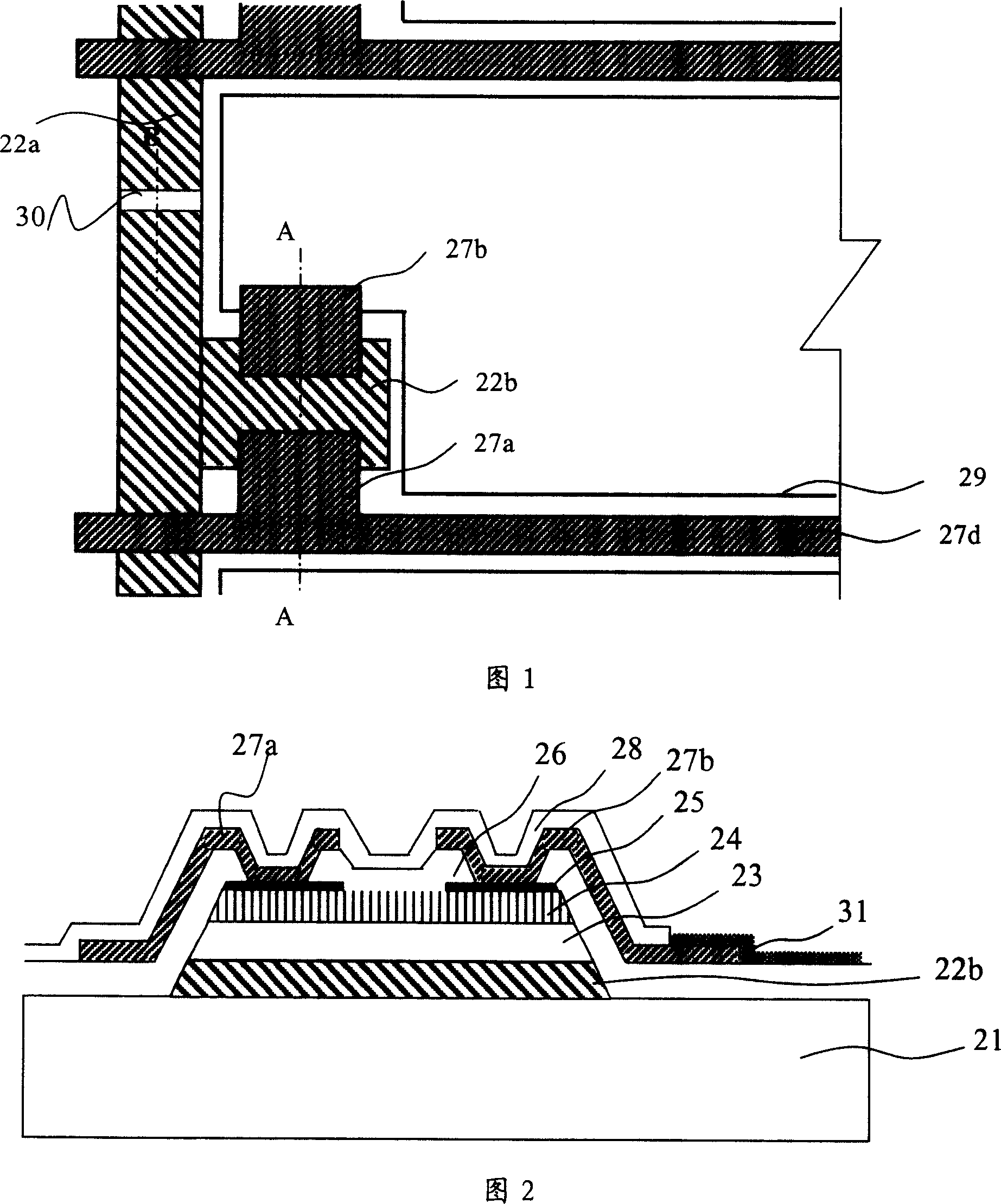
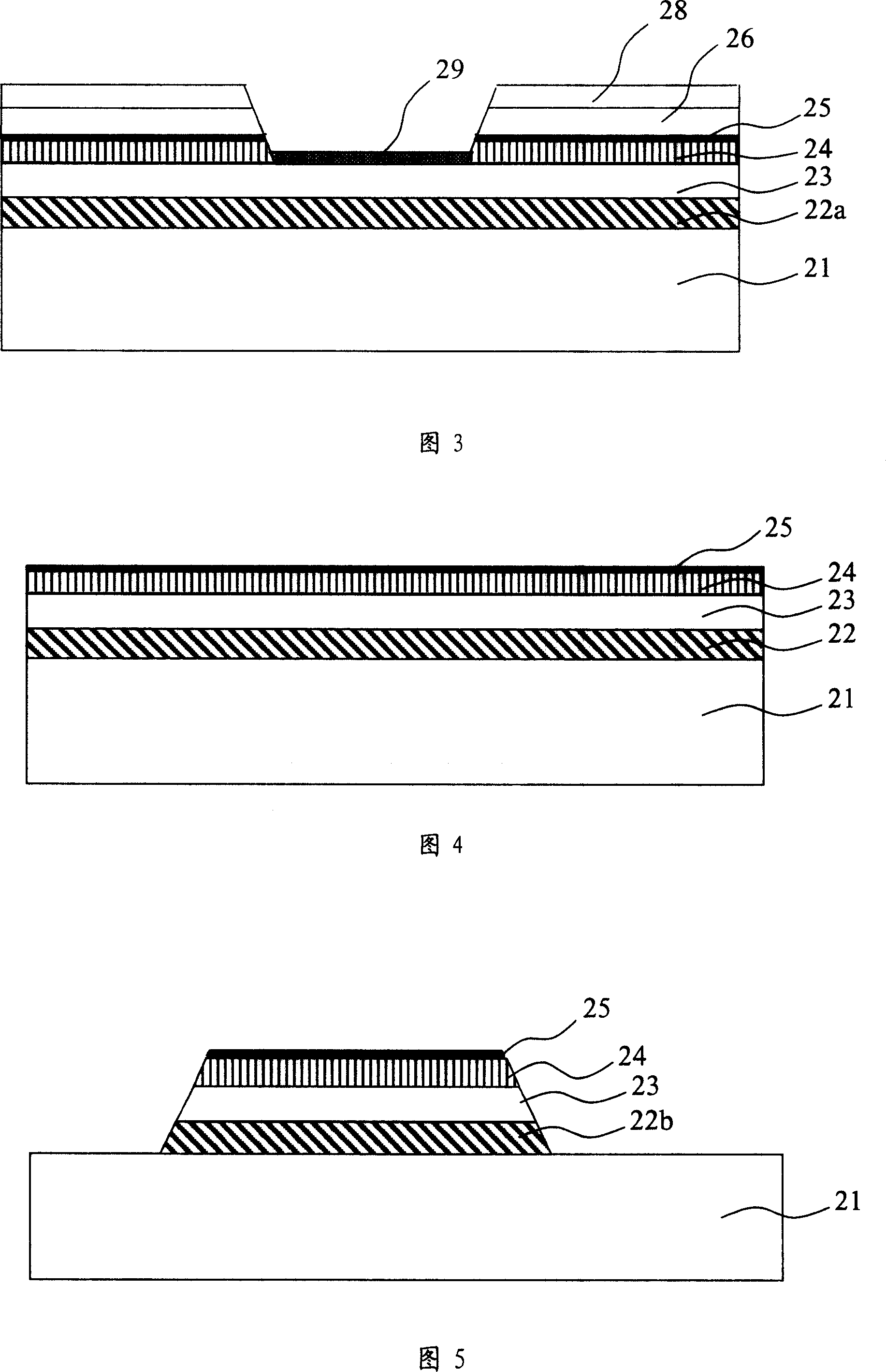
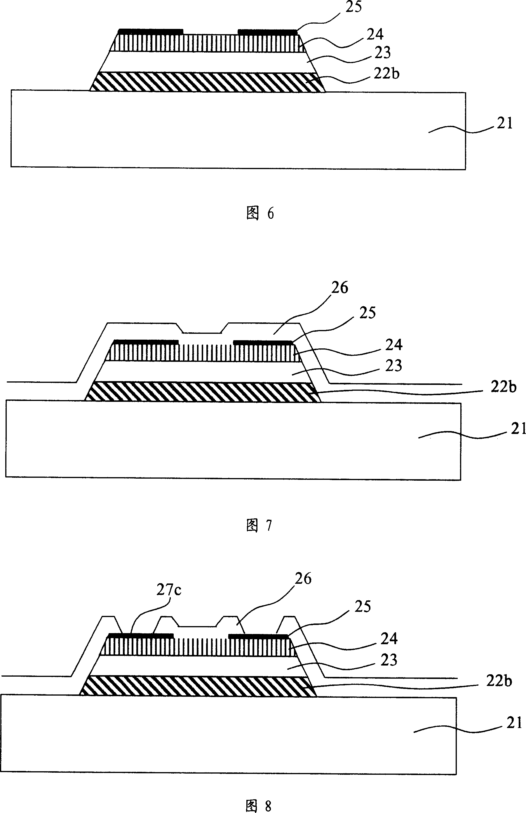
[0038] Fig. 1, Fig. 2 and Fig. 3 show the structure of the TFT matrix of the present invention.

[0039] As shown in Fig. 1, Fig. 2 and Fig. 3, the TFT matrix structure of the present invention comprises: a substrate 21; a gate line 22a and an integral gate electrode 22b formed on the substrate 21; above the gate line 22a and the gate electrode 22b Covered with a first layer of insulating layer 23, a semiconductor layer 24 and an ohmic contact layer 25 in sequence; the TFT channel is formed on the ohmic contact layer 25 on the gate electrode 22b; the second layer of gate insulating layer 26 is formed on the ohmic contact layer 25 the source-drain electrode via hole 27c is formed on both sides of the channel of the thin film transistor; the data line 27d and the source electrode 27a integrated with it are formed on the top of the second insulating layer 26, and pass through the source-drain electrode via hole 27c and the gate The ohmic contact layer 25 on the electrode 22b is c...


PUM


Abstract

The invention discloses a TFT array structure, which comprises a substrate; a gate line and a gate electrode; a first insulating layer, a semi-conductive layer and an ohmic contact layer which are covered in order on the gate line and the gate electrode; a thin film transistor (TFT) groove; a second insulating layer formed on the ohmic contact layer; a source/drain electrode through hole formed on the second insulating layer; data lines and a source electrode integrated with the data lines and connected with the ohmic contact layer on the gate electrode; a drain electrode connected with the ohmic contact layer on the gate electrode; a passivation layer formed on the data lines, the source electrode and the drain electrode; a pixel electrode formed on the second insulating layer and partially lapped on the drain electrode; and a groove formed on the gate line between the data lines to cut off the ohmic contact layer on the gate line. The invention also discloses a fabrication method of the array structure. The inventive array structure and the fabrication method thereof shorten the production cycle of the TFT array and reduce the production cost.

Description

technical field [0001] The invention relates to a thin film transistor (TFT) matrix structure and a manufacturing method thereof, in particular to a TFT matrix structure prepared by four photolithography and a manufacturing method thereof. Background technique [0002] Liquid crystal display mode is the mainstream of flat panel display at present, and active drive TFT LCD (thin film transistor liquid crystal display) is the dominant display mode in the field of liquid crystal display. The manufacturing process of TFT LCD is compatible with traditional IC circuits. It has excellent display quality, low power consumption, light weight, and no radiation. It is a very friendly human-machine communication interface. Its main application fields are notebook computers and desktop computer monitors. , workstations, industrial monitors, global satellite positioning system (GPS), personal data processing, game consoles, videophones, portable VCD, DVD and other portable devices. [00...

Claims


Application Information

Patent Timeline
Patent Type & Authority Applications(China)
IPC IPC(8): H01L27/12H01L21/84G02F1/136
Inventor 王章涛邱海军闵泰烨林承武
Owner BEIJING BOE OPTOELECTRONCIS TECH CO LTD
Why Eureka
Try Eureka