A method for obtaining low bit discrepancy density extension thin film via using neck down extension

An epitaxial thin film, low dislocation technology, used in electrical components, semiconductor/solid-state device manufacturing, circuits, etc., can solve the problems of high cost, thick buffer layer, poor compatibility, etc., and achieve the effect of good surface roughness

Inactive Publication Date: 2008-03-26
JIANGXI SORNID HI TECH
View PDF0 Cites 22 Cited by
  • Summary
  • Abstract
  • Description
  • Claims
  • Application Information

AI Technical Summary

Problems solved by technology

The disadvantage of this method is that in order to obtain a surface layer film with low dislocation density, the thickness of the buffer layer is required to be very thick. Generally, the thickness of the buffer layer required to deposit germanium on silicon is about 10um.
Such a thick structure is expensive and not compatible with traditional CMOS processes
[0006] Another method is to use high temperature 900°C annealing to perform cyclic annealing on the film, which can make the screw dislocation slide. When the screw dislocation slides to the boundary of the film or when the two dislocation lines cancel each other out, the dislocation in the film However, the best results reported using this method are not as good as those using a graded buffer layer, and , multi-step high-temperature annealing will adversely affect other devices that have been formed in the integrated circuit

Method used


Image

  • A method for obtaining low bit discrepancy density extension thin film via using neck down extension
  • A method for obtaining low bit discrepancy density extension thin film via using neck down extension

Examples


Embodiment Construction

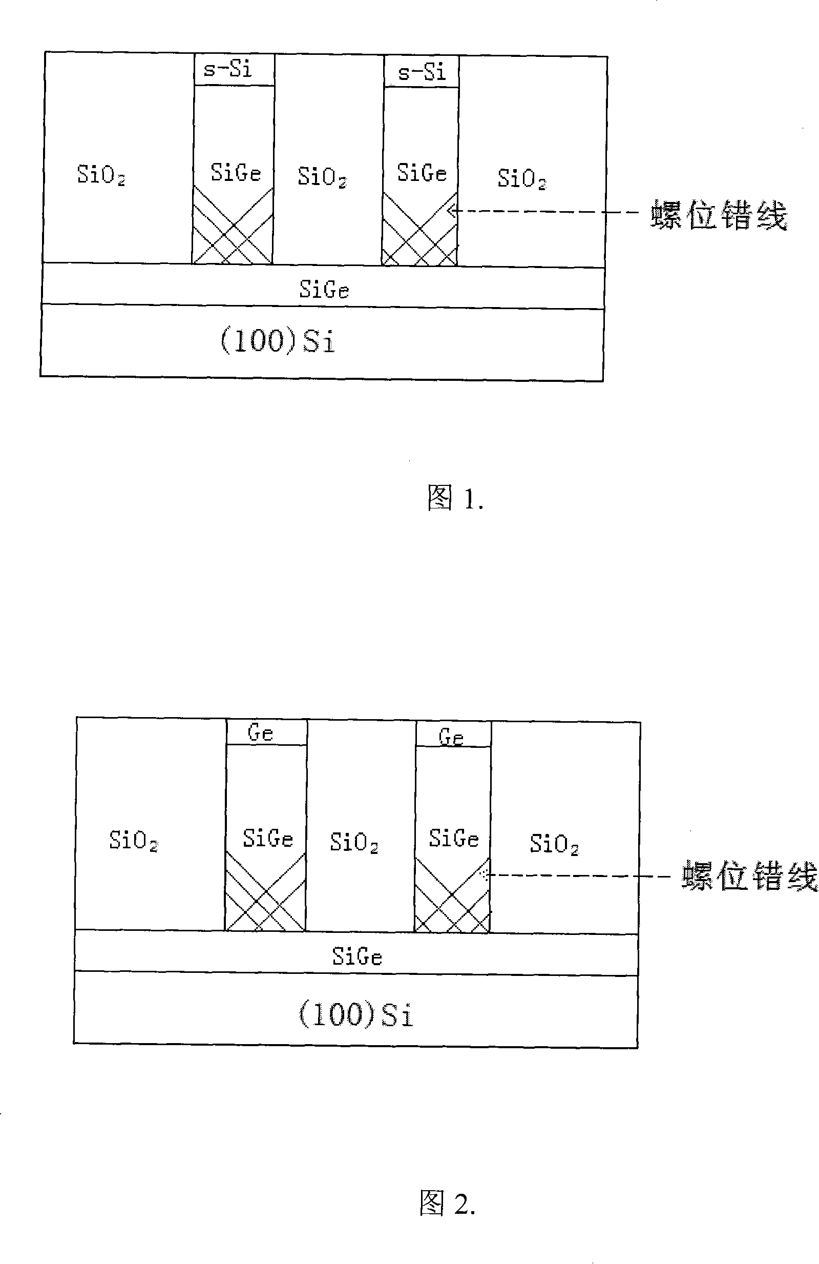
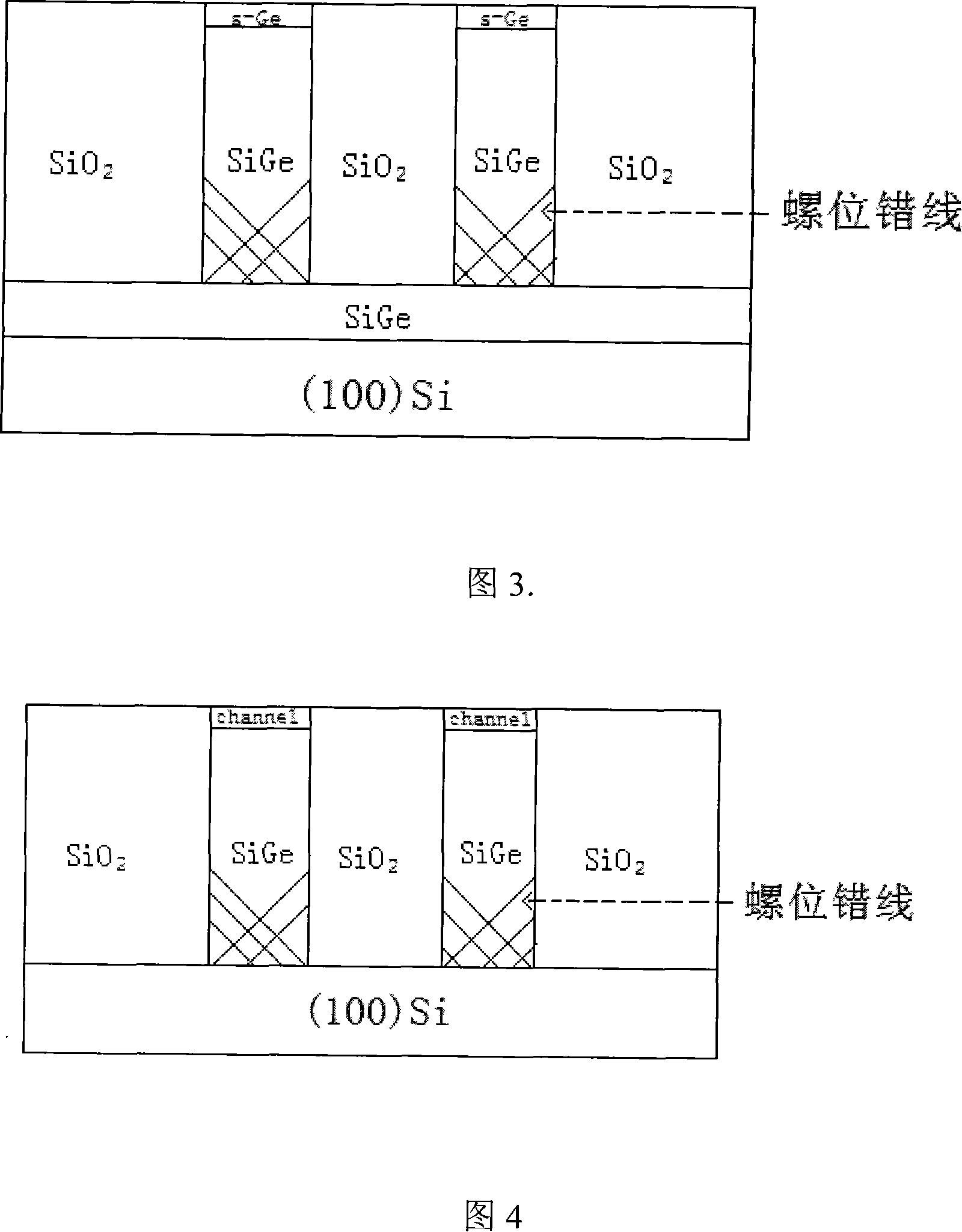
[0037] The invention provides a method for obtaining epitaxial film with low dislocation density by using neck-in epitaxy. The method uses the preparation methods of deposition, selective epitaxy and thermal oxidation to manufacture a silicon germanium substrate with low dislocation density and a channel with high mobility.

[0038] 1-3 are schematic cross-sectional views of growing strained silicon, germanium, and strained germanium channel structures on silicon germanium substrates, respectively. The manufacturing process of these three structures is: first deposit a layer of silicon germanium with low germanium content on the surface of the silicon wafer, oxidize the silicon germanium layer to increase the proportion of germanium in it; grow thick silicon germanium on the concentrated silicon germanium Silicon dioxide layer, photolithography and etching this layer of silicon dioxide to obtain a series of hole structures, and the bottom of the hole is a silicon germanium lay...


PUM


Abstract

This invention discloses a method for using necking extension to get extension films of low dislocation density, which utilizes deposition, selective extension and thermal oxidation to prepare GeSi substrates of low dislocation density and channels of high migration rate and gets films of exremely low dislocation density on a silicon wafer meeting the requirement of MOS devices or luminescent devices.

Description

technical field [0001] The invention belongs to the technical field of semiconductor material preparation, and in particular relates to a method for obtaining a low dislocation density epitaxial film by necking down epitaxy. Background technique [0002] Using some new materials in CMOS devices or optoelectronic devices can improve the performance of the devices. For example, using germanium, strained silicon, or strained germanium as a new channel material can reduce the effective mass of carriers in the channel, thereby increasing their mobility, which is an important direction to make MOSFETs adapt to the trend of scaling down the size of transistors ; The band gap of germanium is small, which is suitable for making optoelectronic devices. In order to apply the existing traditional CMOS technology, various new materials need to be fabricated on the silicon substrate, which brings a series of problems. [0003] For strained silicon channels, in order to achieve the strai...

Claims


Application Information

Patent Timeline
IPC IPC(8): H01L21/20
Inventor 赵硕梁仁荣刘佳磊王敬徐洋刘志弘许军
Owner JIANGXI SORNID HI TECH
Why Eureka
Try Eureka