Film transistor and its making method

A technology of thin film transistor and manufacturing method, which is applied in the direction of transistor, semiconductor/solid-state device manufacturing, semiconductor device, etc., can solve problems such as ion diffusion, and achieve the effect of improving bonding strength, improving ion diffusion problem, and reducing copper layer peeling.

Inactive Publication Date: 2008-05-14
CHUNGHWA PICTURE TUBES LTD
View PDF0 Cites 16 Cited by
  • Summary
  • Abstract
  • Description
  • Claims
  • Application Information

AI Technical Summary

Problems solved by technology

[0004] The invention provides a method for manufacturing a

Method used


Image

  • Film transistor and its making method
  • Film transistor and its making method
  • Film transistor and its making method

Examples


Embodiment Construction

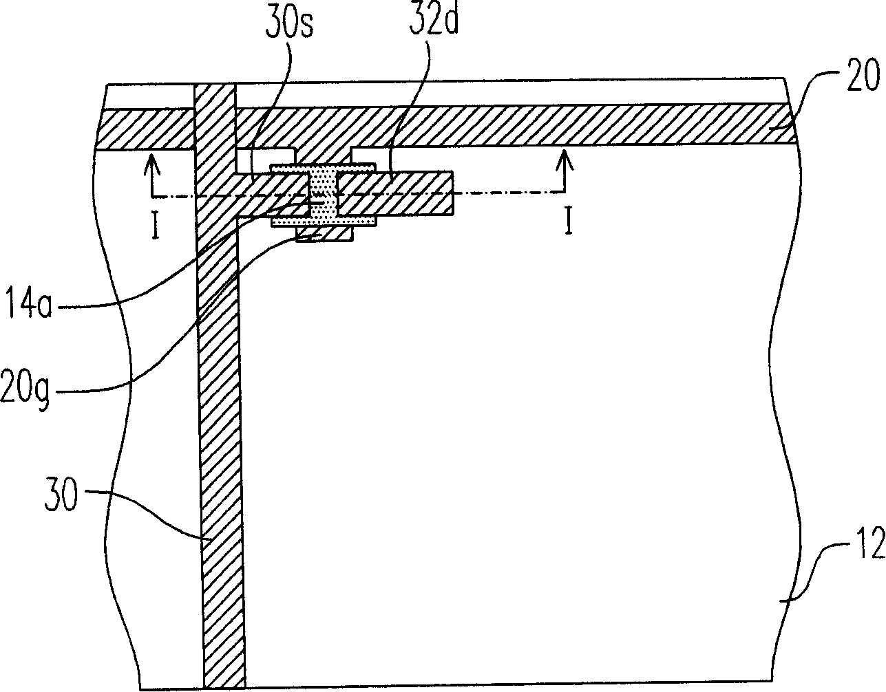
[0026] In view of the shortcomings of the prior art, the present invention proposes to use a double-layer structure of nitrogen-containing copper alloy layer / copper layer as the gate, source and drain of the thin film transistor, so as to improve the phenomenon of copper diffusion and increase the copper pair Silicon adhesion.

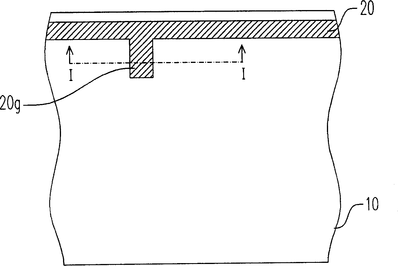
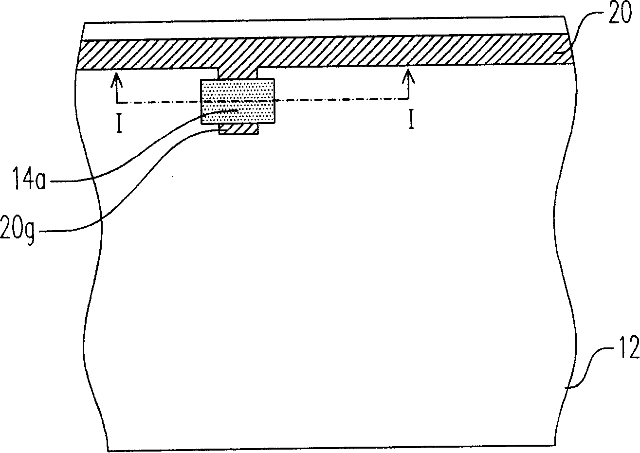
[0027] Figure 1A to Figure 1D It is a top view of the manufacturing process of a thin film transistor according to an embodiment of the present invention; Figure 2A to Figure 2D are along Figure 1A to Figure 1D Sectional drawing of section line I-I. Figure 1A to Figure 1D The range shown is the range of a pixel structure of a thin film transistor array substrate (TFT array substrate). Use the following first Figure 1D and Figure 2D Next, the thin film transistor of the present invention will be described, and then its manufacturing method will be described.

[0028] Please also refer to Figure 1D and Figure 2D , The thin film transistor of...


PUM

PropertyMeasurementUnit
Thicknessaaaaaaaaaa
Thicknessaaaaaaaaaa

Abstract

The invention discloses a thin film transistor and a manufacturing method thereof. Firstly, a gate is formed on a substrate. Then, a gate insulation layer is formed to cover the gate, and a channel layer is formed on the part of the gate insulation layer upon the gate. Later, a source and a drain are formed on the channel layer. The method for forming the gate comprises can be that a nitrogen-containing copper alloy layer and a copper layer are orderly formed and the nitrogen-containing copper alloy layer and the copper layer are partially removed. The method for forming the source and drain can be the same.

Description

technical field [0001] The present invention relates to an active element and its manufacturing method, and in particular to a thin film transistor and its manufacturing method. Background technique [0002] In the internal wiring of a general liquid crystal display panel, metals such as molybdenum, tantalum, chromium, tungsten or their alloys are generally used as the material of the metal layer, and aluminum is the most commonly used. However, copper has less electromigration problems and has low resistivity than aluminum, so copper has become a very attractive research and development topic in recent years. [0003] However, there are practical difficulties with copper interconnects. Copper has poor thermal stability. For example, in the manufacturing process of thin film transistors, the copper used as the gate is easily melted due to high temperature, and then diffuses and crosses the interface between copper and silicon or the interface between copper and silicon dio...

Claims


Application Information

Patent Timeline
IPC IPC(8): H01L21/336H01L21/28H01L29/786H01L29/43
Inventor 赖钦诠邱羡坤林宜平杨淑贞
Owner CHUNGHWA PICTURE TUBES LTD
Why Eureka
Try Eureka