Graded hybrid amorphous silicon nanowire solar cells

A technology of amorphous layer and nanohole, applied in nanotechnology, circuits, electrical components, etc., can solve problems such as reducing device performance

Inactive Publication Date: 2008-05-21
GENERAL ELECTRIC CO
View PDF7 Cites 16 Cited by
  • Summary
  • Abstract
  • Description
  • Claims
  • Application Information

AI Technical Summary

Problems solved by technology

These defects can act as sites for charge carrier recombination that degrades device performance

Method used


Image

  • Graded hybrid amorphous silicon nanowire solar cells
  • Graded hybrid amorphous silicon nanowire solar cells
  • Graded hybrid amorphous silicon nanowire solar cells

Examples


Embodiment 1

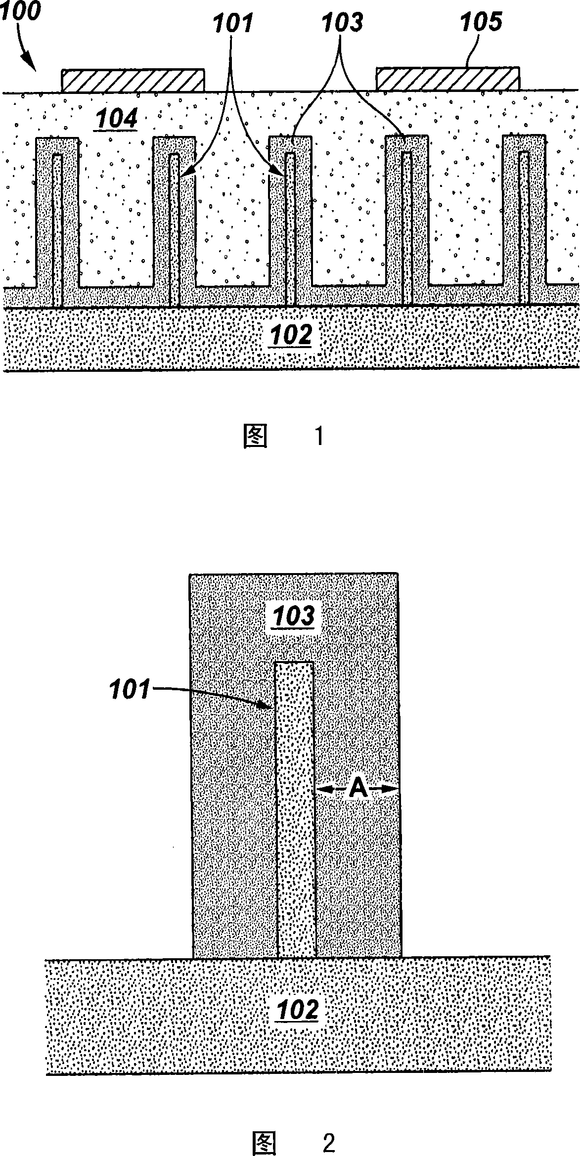
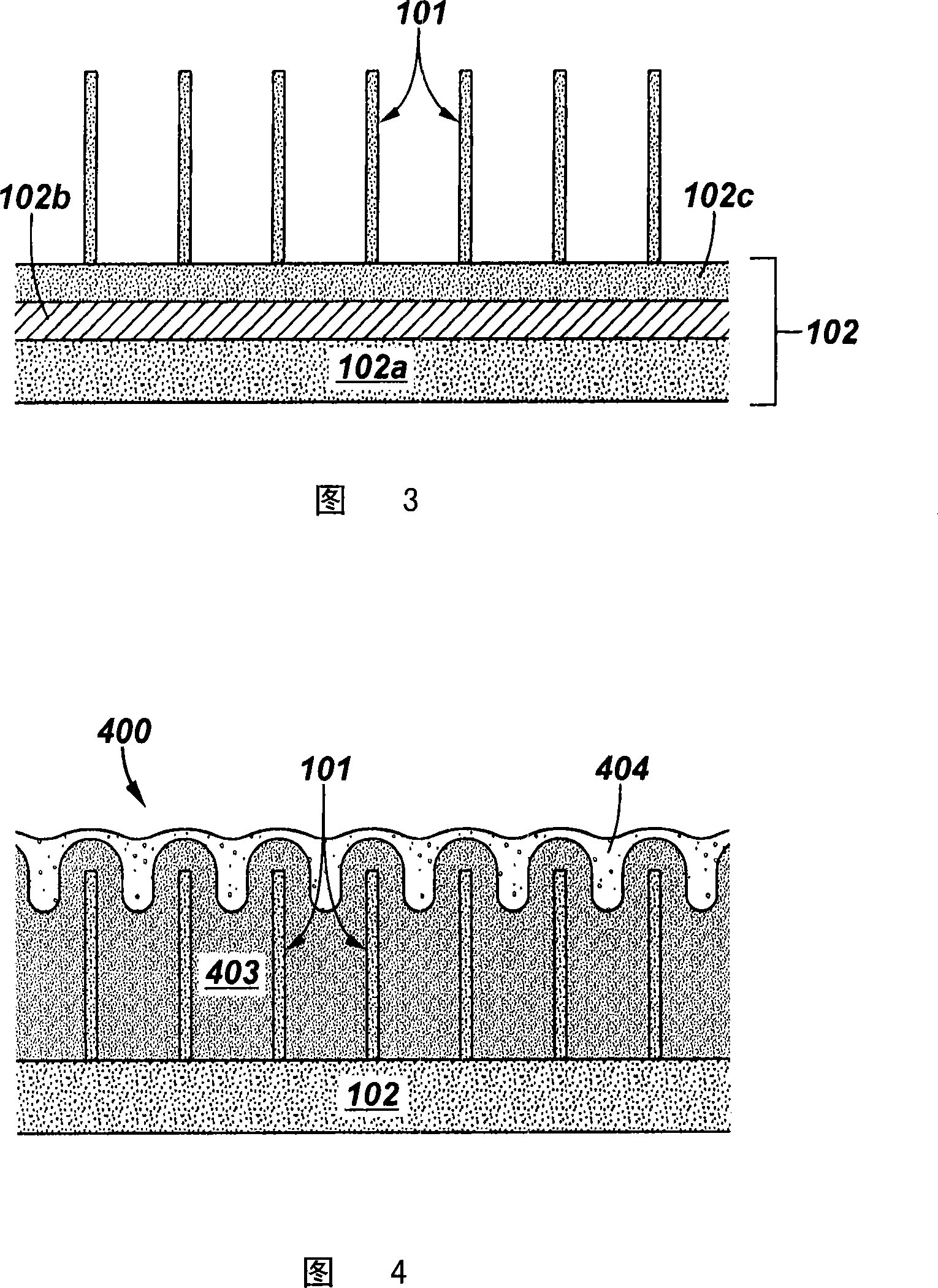
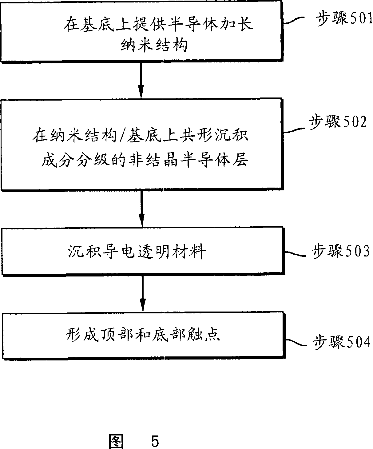
[0077] This example serves to demonstrate the process steps for fabricating compositionally graded hybrid nanowire optoelectronic devices according to certain embodiments of the present invention.

[0078] A film of silicon nanowires of one conductivity type on a glass, metal or semiconductor substrate is disposed in a plasma reaction chamber (eg, a plasma enhanced chemical phase deposition system). A vacuum pump removes the atmosphere from the chamber. The substrate to be treated is preheated to 120-240°C. A hydrogen plasma surface preparation step is performed prior to the deposition of the compositionally graded layer. H 2Introduce into the chamber at a flow rate of 50-500 sccm (standard cubic centimeters per minute). A throttle valve was used to maintain a constant process pressure in the range of 200-800 mTorr. The power density is 6-50mW / cm 2 A range of AC frequency input power is used to energize and maintain the plasma. The applied input power can be from 100kHz ...

Embodiment 2

[0083] This example serves to demonstrate illustrative applications in which optoelectronic device 100 (or variations thereof) may be used in accordance with certain embodiments of the present invention.

[0084] A photovoltaic module comprising a plurality of photovoltaic devices 100 is typically installed on a residential roof for grid-connected power generation. The modules are installed in several ways to achieve functional and sensory quality. The module now uses standard residential solar modules to provide electricity that can be stored or sold back to the utility for revenue. These solar cells can be cut to standard sizes and mounted into module frames, connected in series using standard solder-based interconnection methods, in some cases with bypass diodes to minimize shadowing effects. The all-glass substrate can be used directly in a framed module where the nanowires are grown on a transparent material, or the glass can be laminated and used as a module that does n...


PUM

PropertyMeasurementUnit
thicknessaaaaaaaaaa
lengthaaaaaaaaaa
widthaaaaaaaaaa

Abstract

The present invention is directed to compositionally-graded hybrid nanostructure-based photovoltaic devices comprising elongated semiconductor nanostructures and an amorphous semiconductor single layer with continuous gradation of doping concentration across its thickness from substantially intrinsic to substantially conductive. In other embodiments, the present invention is directed to methods of making such photovoltaic devices, as well as to applications which utilize such devices (e.g., solar cell modules).

Description

technical field [0001] The present invention relates generally to optoelectronic devices, and in particular to such optoelectronic devices comprising elongated silicon nanostructures as active elements within the device. Background technique [0002] Silicon (Si) is now the most commonly used material in the manufacture of solar cells that can be used to convert sunlight into electricity. For this purpose, single p-n junction as well as multiple p-n junction solar cells are used, but these are not effective enough to significantly reduce the costs involved in the production and use of this technology. Therefore, the competition of conventional power sources precludes the general use of this solar cell technology. [0003] The initial depletion process of existing solar cells occurs when light-excited electrons rapidly lose any energy they may have beyond the energy band due to interactions with lattice vibrations (already known as phonons) Gaps, leading to increased recomb...

Claims


Application Information

Patent Timeline
Patent Type & Authority Applications(China)
IPC IPC(8): H01L31/042H01L31/0352H01L31/06H01L31/20H01L31/065
CPCH01L31/0352H01L31/065Y02E10/50H01L31/074B82Y40/00H01L31/04H01L31/18
Inventor L·察卡拉科斯J·N·约翰逊V·马尼文南
Owner GENERAL ELECTRIC CO
Why Eureka
Try Eureka