A making method of EEPROM for increasing coupling voltage of float grating

A technology of coupling voltage and manufacturing method, which is applied in the manufacturing of circuits, electrical components, semiconductor/solid-state devices, etc., and can solve problems such as operating voltage and erasing and writing rate limitations.

Active Publication Date: 2008-05-28
SHANGHAI HUAHONG GRACE SEMICON MFG CORP
View PDF0 Cites 1 Cited by
  • Summary
  • Abstract
  • Description
  • Claims
  • Application Information

AI Technical Summary

Problems solved by technology

In EEPROM (electrically erasable programmable read-only memory), in order to ensure the reliability of the cell (EEPROM storage unit), ONO (that is, oxide-nitride-oxide, oxide film nitride film oxide film sandwich structure, ONO is mainly used in In EEPROM, FLASH, and DRAM processes, as an insulating layer, it has the advantages of small leakage and few defects), and the thickness cannot be reduced a lot, so the operating voltage and erasing rate are limited to a certain extent.

Method used


Image

  • A making method of EEPROM for increasing coupling voltage of float grating
  • A making method of EEPROM for increasing coupling voltage of float grating
  • A making method of EEPROM for increasing coupling voltage of float grating

Examples


Embodiment 1

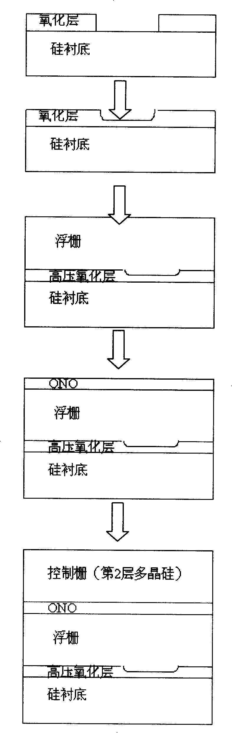
[0017] Such as figure 2 Shown is a specific embodiment of the method of the present invention.

[0018] Such as figure 2 , same as the production of the usual EEPROM, in this embodiment, a high-voltage oxide film is first grown, and then tunnel etching is performed; then a layer of 80A tunnel oxide is grown; and a layer of 1500A floating poly is grown; this embodiment and the traditional method The difference is that a step is added at this time, that is, floating gate etching. In this case, it is to dig a hole on the tunnel window; then grow ONO with a thickness of 60 / 60 / 60A (angstroms); then grow Poly2, The thickness is 2000A; the next steps are the same as the usual EEPROM production method.

Embodiment 2

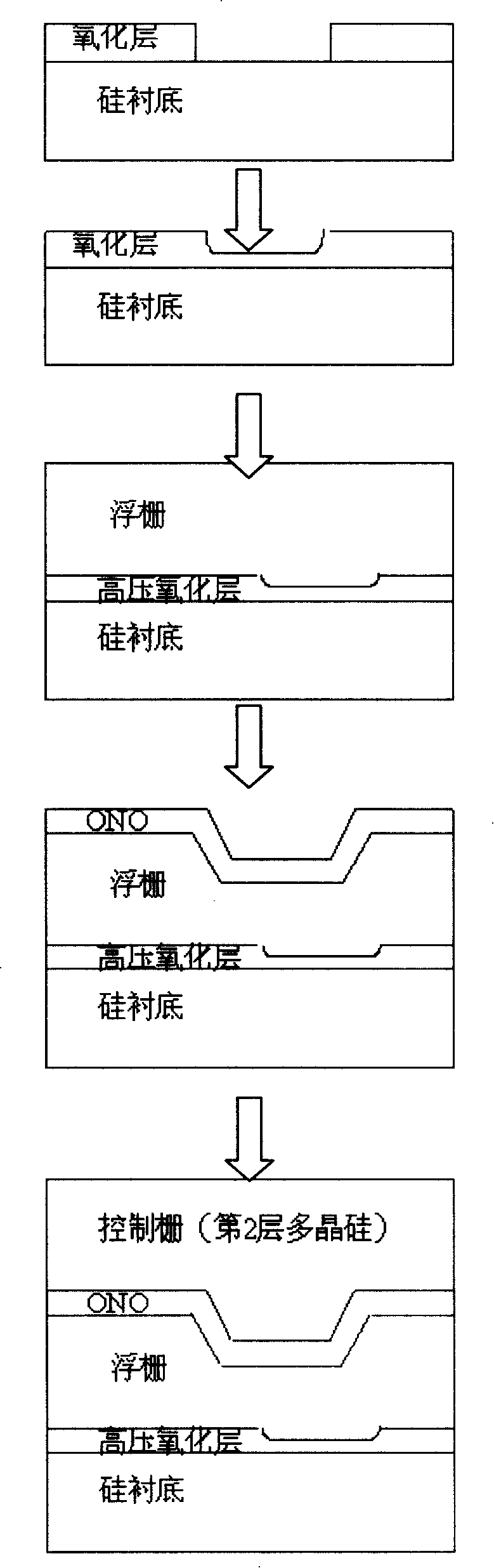
[0020] Such as image 3 Shown is another specific embodiment of the method of the present invention.

[0021] This example is the same as figure 2 The most important difference of the shown embodiment is that the etching pattern of the floating gate is different. In the above example, a hole is dug on the tunnel window, but in this example, the poly on the tunnel window is retained, and the poly next to it is dug out.

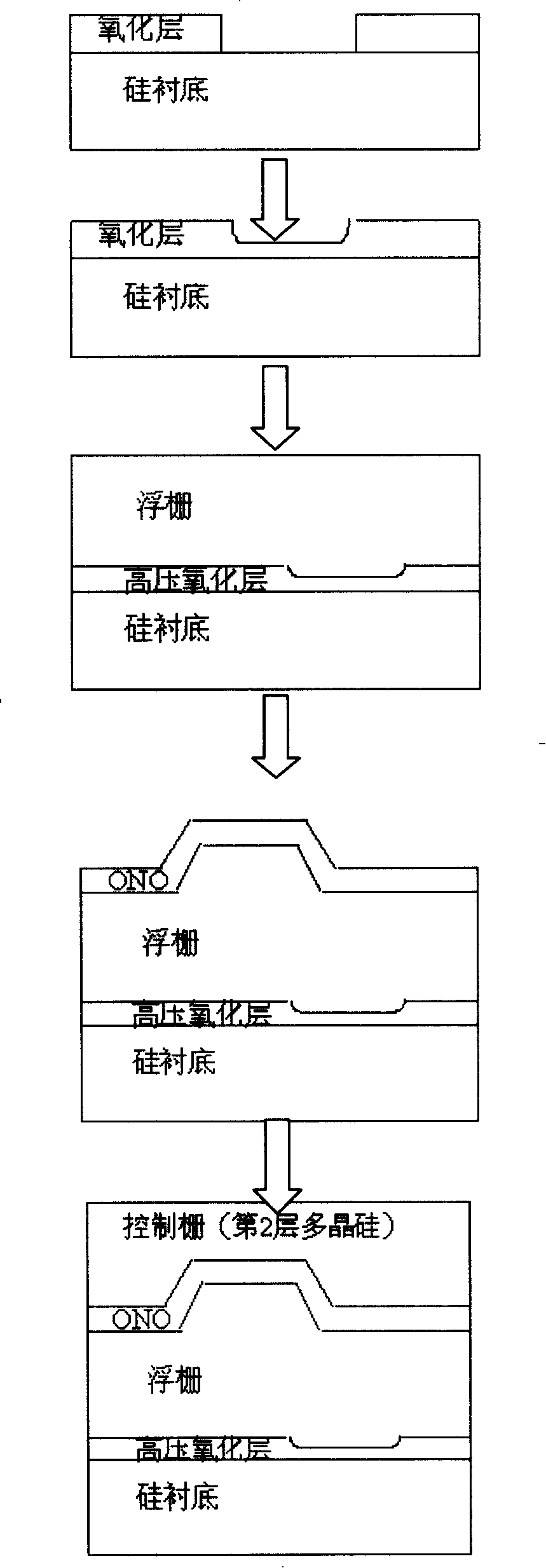
[0022] Image 6 It is the effect comparison diagram of the inventive method and the traditional method, wherein Fig. a is the usual EEPROM storage unit structure under the traditional method, and Fig. b is figure 2 The structure of the EEPROM memory cell with increased floating gate etching shown in Figure c is image 3 Shown is the EEPROM memory cell structure with increased floating gate etching.

[0023] Next, let's compare the ONO capacitance and erase / write coupling ratio of the EEPROM Cell after adding an EEPROM floating gate etching (including diff...


PUM


Abstract

The invention discloses an EEPROM manufacture method which can increase the floating gate coupling voltage. The method besides includes steps of growing a high voltage oxide film, carrying out channel etching, growing a layer of channel oxides, growing a layer of floating gate polycrystals, growing a ONO, and growing two layers of the polycrystals; the floating gate etching is carried out after growing a layer is carried out and before growing the ONO is carried out. A pattern of the floating gate etching is composed of a cubic block or a plurality of small cubic blocks. Because the invention increases one time floating gate etching and the capacitance of the ONO in a traditional EEPROM manufacture method, that is, the coupling ratio and the coupling voltage of the floating gate are increased, the recordable efficiency of the EEPROM can be enhanced or the recordable voltage is decreased.

Description

technical field [0001] The invention relates to a semiconductor manufacturing process, in particular to an EEPROM manufacturing method capable of increasing the coupling voltage of a floating gate. Background technique [0002] At present, with the increasing development of semiconductor manufacturing technology, especially in the design of memory cells, in order to improve competitiveness, it is necessary to reduce the cell area as much as possible and simplify the manufacturing process. In EEPROM (electrically erasable programmable read-only memory), in order to ensure the reliability of the cell (EEPROM storage unit), ONO (that is, oxide-nitride-oxide, oxide film nitride film oxide film sandwich structure, ONO is mainly used in In EEPROM, FLASH, and DRAM processes, as an insulating layer, it has the advantages of small leakage and few defects), and the thickness cannot be reduced a lot, so the operating voltage and erasing rate are limited to a certain extent. Contents ...

Claims


Application Information

Patent Timeline
Patent Type & Authority Applications(China)
IPC IPC(8): H01L21/28H01L21/336H01L21/8247
Inventor 孙亚亚龚顺强
Owner SHANGHAI HUAHONG GRACE SEMICON MFG CORP
Why Eureka
Try Eureka