Production method of LED chip for illumination

A technology of LED chip and manufacturing method, which is applied in the direction of electrical components, circuits, semiconductor devices, etc., can solve problems such as difficult to overcome LED chip defects, difficult product integration, and complicated packaging process, so as to improve LED light output rate and reduce total reflection loss, the effect of encapsulation process simplification

Inactive Publication Date: 2008-06-11
JIANGSU ALLRAY
View PDF0 Cites 8 Cited by
  • Summary
  • Abstract
  • Description
  • Claims
  • Application Information

AI Technical Summary

Problems solved by technology

The disadvantages of LED chips produced by this method are: (1) the packaging process is relatively complicated, and the light output rate is low; (2) the product is difficult to miniaturize; (3) the product is not easy to integrate
In order to improve the luminous performance of LED lamps for lighting, the common practice in the industry is to achieve good luminous effect by improving the packaging process, but it is difficult to overcome the defects of LED chips under the current packaging process

Method used


Image

  • Production method of LED chip for illumination
  • Production method of LED chip for illumination
  • Production method of LED chip for illumination

Examples


Embodiment Construction

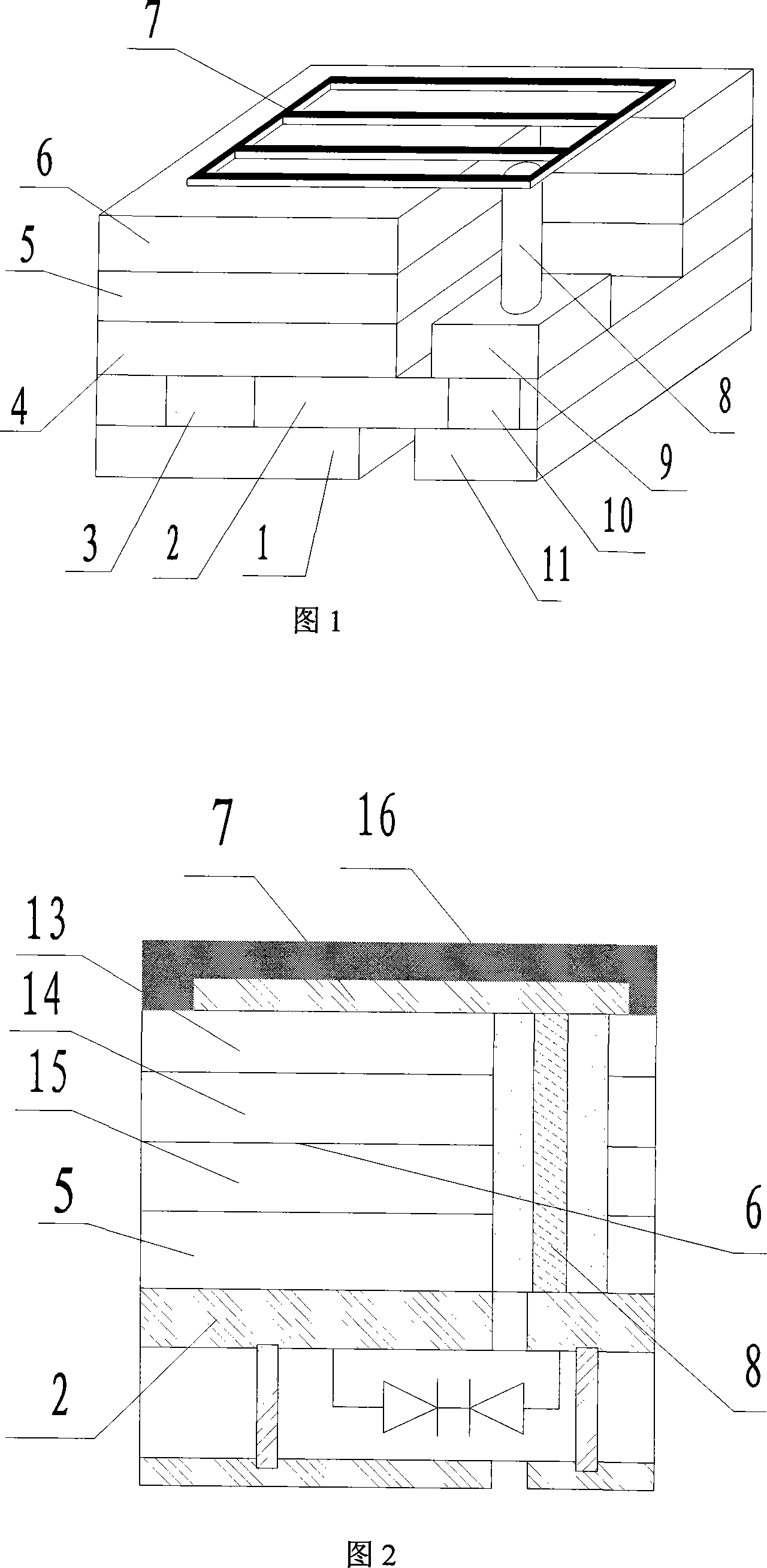
[0019] Firstly, a blue LED chip with a vertical through-hole structure is fabricated, as shown in FIG. 1 , an LED epitaxial layer 6 and a metallized silicon support substrate 2 with an antistatic diode are prepared. The LED epitaxial layer 6 includes GaN-based LED epitaxial wafers (polarized and non-polarized), GaP-based LED epitaxial wafers, ZnO-based LED epitaxial wafers, or epitaxial wafers of other semiconductor devices. For GaP-based LEDs, GaN-based LEDs, ZnO-based LEDs or other semiconductor devices. Different growth substrate materials are used, for example, GaAs growth substrate, GaP growth substrate, sapphire growth substrate, silicon carbide growth substrate, ZnO growth substrate, silicon growth substrate, compound GaN-based growth substrate, compound ZnO base growth substrate, etc. The epitaxial layer 6 of the LED is bonded to the metallized silicon support substrate 2 with antistatic diodes. Bonding methods include conductive glue, metal melting, metal diffusion,...


PUM


Abstract

The invention discloses a manufacture method for lighting LED chip. A LED chip of vertical via structure is manufactured by common methods; epitaxial layers of the chip comprise the first-type confinement layer, an activated layer and the second-type confinement layer; a transparent layer is grown on the first-type confinement layer, surface of the transparent layer etched, and prismatic micro-lens array developed; the prismatic micro-lens array layer and the epitaxial layer are etched around the epitaxial layer until the upper surface of the reflection/ohm/bonding layer exposed, and a groove formed at the outer circle; the fluorescent powders layers are formed on the surface of the prismatic micro-lens array and inside the groove. The epitaxial layer is cut into chips and packed; when packing LED by the chips, no fluorescent powders coating is needed; white light can be emitted directly and the packing process greatly simplified; exit surface is changed from planar to spherical surface, which greatly reduces total reflection and improves the light extracting rate of LED; the invention can be easily integrated and miniaturized.

Description

technical field [0001] The invention relates to a semiconductor light emitting diode (LED) light source, in particular to a method for manufacturing a white LED chip in the lighting field. Background technique [0002] Light-emitting diode (LED) is a new type of light source. Compared with traditional light sources, it has many advantages: longevity, energy saving, low voltage, small size, and no pollution. Since the birth of LED, the technology has been continuously improving, and the luminous efficiency has been continuously improved. At present, the luminous efficiency of white LED has surpassed that of ordinary fluorescent lamps, and LED has begun to enter the field of lighting. [0003] At present, the LED chip with vertical through-hole structure is the most advanced LED chip. As shown in Figure 1, it is a schematic diagram of a typical LED chip with a vertical through-hole structure. Composite layer 5, metal layer 4, support substrate 2 and electrodes 1,11. The epit...

Claims


Application Information

Patent Timeline
Patent Type & Authority Applications(China)
IPC IPC(8): H01L33/00H01L33/50H01L33/58
Inventor 黄振春陈岭史智青洪从胜傅凡
Owner JIANGSU ALLRAY
Why Eureka
Try Eureka