Device for automatically focusing and leveling

A leveling device and automatic focusing technology, which is applied in the direction of exposure devices, optics, instruments, etc. in the photoplate making process, can solve problems such as vibration difficulties, and achieve the effects of convenient optical path direction, reduced size, and convenient adjustment

Active Publication Date: 2008-06-18
SHANGHAI MICRO ELECTRONICS EQUIP (GRP) CO LTD
View PDF0 Cites 32 Cited by
  • Summary
  • Abstract
  • Description
  • Claims
  • Application Information

AI Technical Summary

Problems solved by technology

However, when the area where the measurement points are distributed is relatively large, the diameter of the required vibration mirror will also incr

Method used


Image

  • Device for automatically focusing and leveling
  • Device for automatically focusing and leveling
  • Device for automatically focusing and leveling

Examples


Embodiment Construction

[0033] The following specific examples illustrate the implementation of the present invention, and those skilled in the art can easily understand other advantages and effects of the present invention from the content disclosed in this specification.

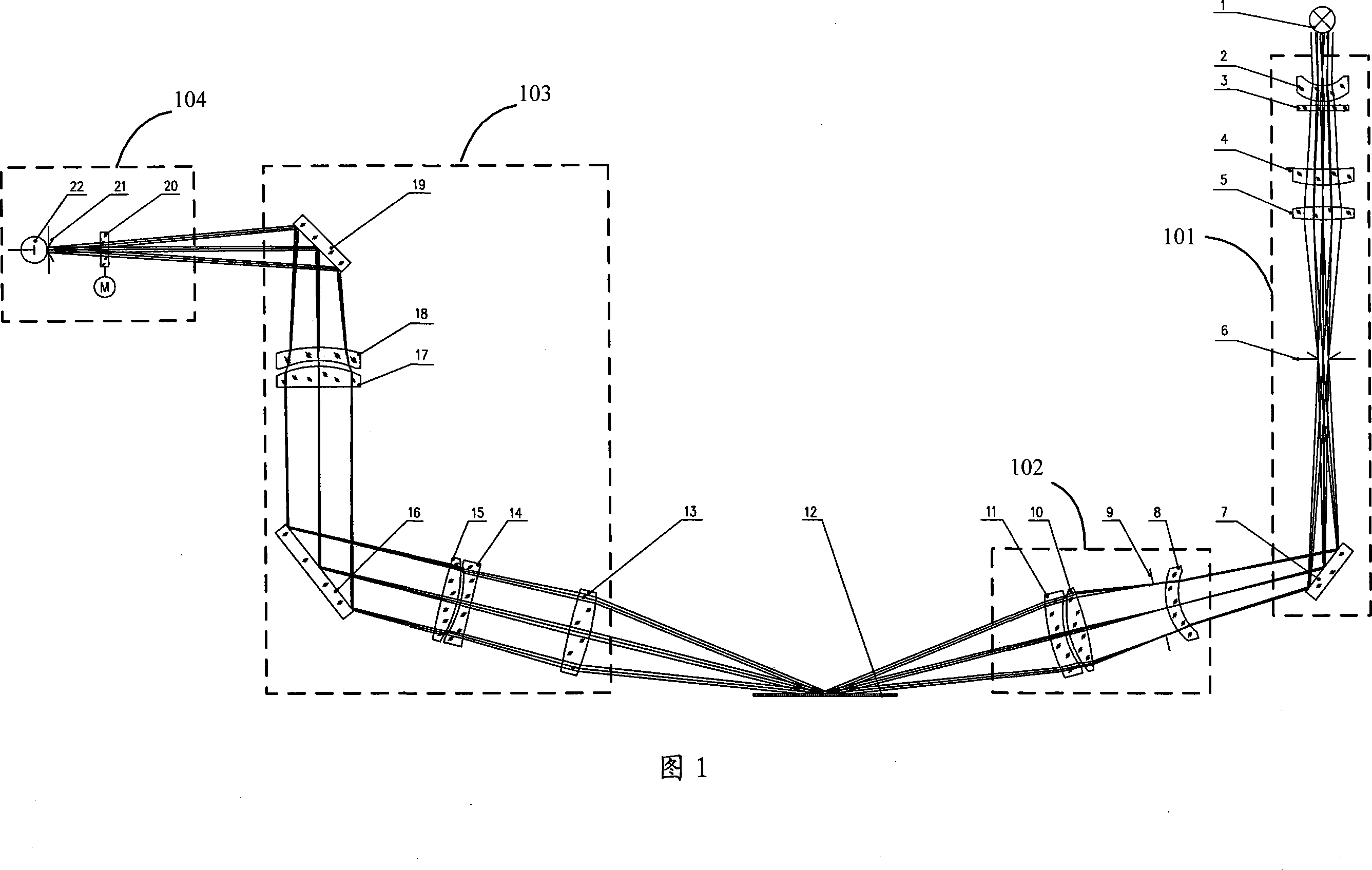
[0034] Hereinafter, each component of the automatic focusing and leveling device of the present invention will be described in detail with reference to FIG. 1.

[0035] As shown in Fig. 1, the light source 1 is the light emitted by the halogen tungsten lamp introduced by the optical fiber. The automatic focusing and leveling device of the present invention has an optical module and a control module (not shown in the figure) that are electrically connected to measure the height and tilt of the surface of the silicon wafer 12 relative to the focal plane of the projection objective, so that the entire exposure During the process, the silicon wafer is at the best focal plane position of the projection objective. The optical module includ...


PUM


Abstract

The invention provides an automatic focusing and leveling device and is applied in a photoetching machine to measure the height value and lean degree of the surface of a silicon chip to be measured relative to the focal plane of a projection objective lens, therefore, the focusing and leveling of the silicon chip can be realized. The automatic focusing and leveling device is provided with an optical module and a control module, both of which are connected with each other through electricity, wherein, the optical module adopts a plate glass and gets rid of limitation of mechanical size, therefore, the invention can realize high-frequency vibration more easily and is easy to be regulated.

Description

Technical field [0001] The invention relates to an automatic focusing and leveling device, in particular to an automatic focusing and leveling device used on a photoetching machine. Background technique [0002] With the vigorous development of the electronics industry, the application of integrated circuits has become more and more extensive, followed by the high precision of its production. The lithography machine is the most critical equipment in all aspects of integrated circuit production. Lithography technology is the basis of large-scale integrated circuit manufacturing and has become the core driving force to promote the development of integrated circuits. Its main function is to image the pattern on the mask on the silicon wafer through exposure. Since the surface of the silicon wafer is coated with photosensitive photoresist, when the pattern on the reticle is imaged on the silicon wafer, the photoresist at the corresponding position will produce a photochemical reactio...

Claims


Application Information

Patent Timeline
IPC IPC(8): G03F7/20G03F9/00G03F9/02
Inventor 李志丹李尧陈飞彪潘炼东葛贵臣张冲肖可云
Owner SHANGHAI MICRO ELECTRONICS EQUIP (GRP) CO LTD
Why Eureka
Try Eureka