
Etching method of radio frequency device thin dielectric substance capacitance

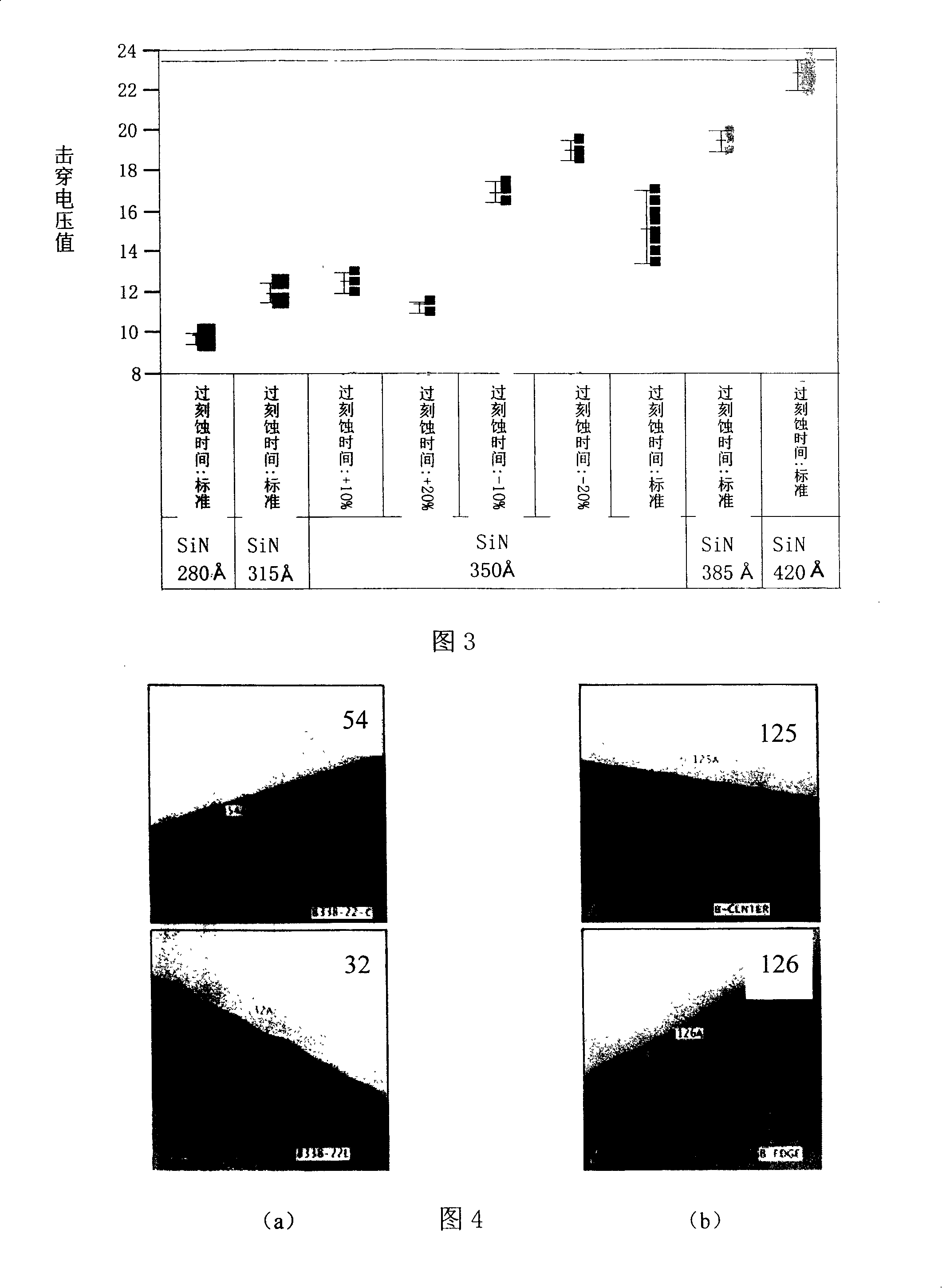
A technology of radio-frequency devices and dielectric materials, which is applied in the manufacture of semiconductor/solid-state devices, circuits, electrical components, etc., can solve the problem of capacitor breakdown voltage drop, achieve the effect of increasing the capacitor breakdown voltage and increasing the remaining thickness

Active Publication Date: 2008-06-18
SHANGHAI HUAHONG GRACE SEMICON MFG CORP
View PDF0 Cites 7 Cited by
  • Summary
  • Abstract
  • Description
  • Claims
  • Application Information

AI Technical Summary

Problems solved by technology

When the thickness of the dielectric silicon nitride is very thin, if the remaining thickness of silicon nitride is too small, the breakdown voltage (BV) of the capacitor will drop

Method used


Image

  • Etching method of radio frequency device thin dielectric substance capacitance
  • Etching method of radio frequency device thin dielectric substance capacitance
  • Etching method of radio frequency device thin dielectric substance capacitance

Examples


Embodiment Construction

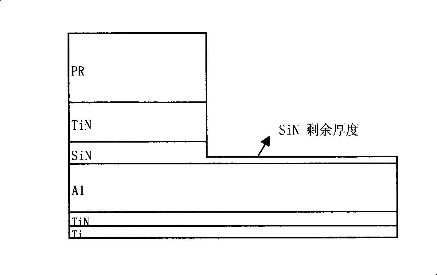
[0021] Such as figure 2 As shown, to make a metal capacitor, the metal titanium nitride should be etched away first, and then stop on the silicon nitride (Si 3 N 4 ) layer, so it is necessary to select corresponding etching conditions for films of different materials.

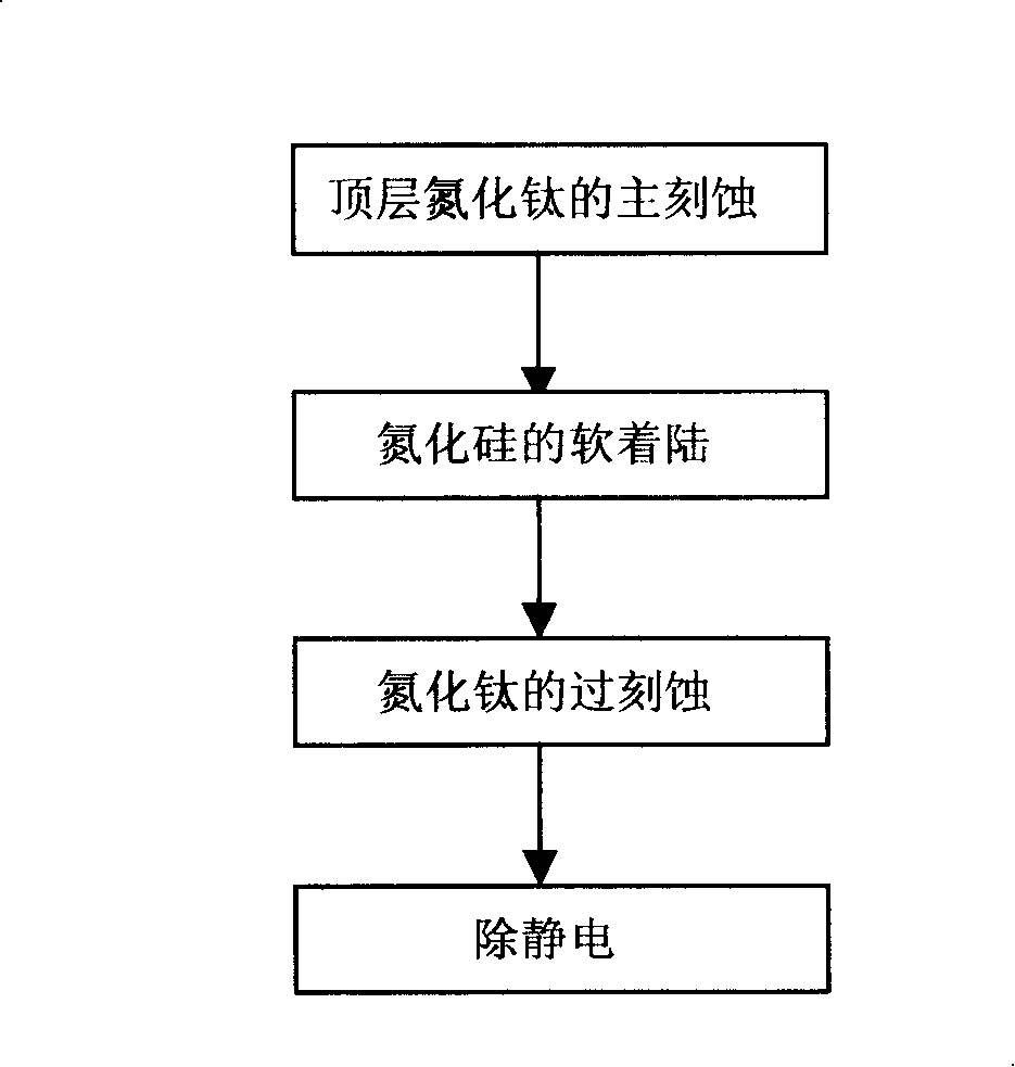
[0022] see figure 1 As shown, the etching process flow of the thin dielectric capacitor of the radio frequency device of the present invention is as follows: after depositing the second layer (aluminum), the dielectric layer (silicon nitride), and the upper electrode (metal titanium nitride) successively, Photoresist is applied, followed by dry etching.

[0023] The first step: the main etching of the top layer of titanium nitride. Considering the requirement of high productivity, high etching rate and low selectivity are used for etching. By controlling the etching time, the etching cannot touch the silicon nitride layer.

[0024] The specific process parameters include: air pressure 6-12 millitorr, upp...


PUM


Abstract

The invention discloses an etching method used for the thin dielectric capacitance of a radio frequency component. The method includes the following steps: firstly, the main etching of a top-layer titanium nitride is carried out and the etching time is controlled to prevent the etching from contacting a silicon nitride layer; secondly, the soft landing of the silicon nitride is carried out and once the etching end point is reached an instant switching to the next step is done; thirdly, the over etching of the titanium nitride is carried out. The invention can overcome the problem that an excessive etching of the dielectric can result in capacitance breakdown and low voltage.

Description

technical field [0001] The invention relates to a manufacturing process method of a semiconductor integrated circuit, in particular to a method for plasma dry etching of capacitors in radio frequency device products. Background technique [0002] In the radio frequency device process, it is necessary to make a metal capacitor (MIM) when doing the second layer of aluminum wiring. That is, after the second layer of aluminum (Al) is deposited, a layer of silicon nitride (SiN) as the dielectric layer and metal titanium nitride (TiN) as the upper electrode are deposited in sequence, and the photoresist (PR) is coated and Exposure, dry etching of silicon nitride. In order to prevent leakage, and considering the process window and process stability, it is required that only half of the silicon nitride can be etched (see figure 2 ). [0003] According to different design requirements, metal capacitors have different sizes and dielectric thicknesses. When the dielectric thickness...

Claims


Application Information

Patent Timeline
IPC IPC(8): H01L21/02H01L21/311H01L21/3213
Inventor 刘鹏吕煜坤
Owner SHANGHAI HUAHONG GRACE SEMICON MFG CORP
Learn More