Method for manufacturing inlaid structure

A manufacturing method and a technology of a mosaic structure, applied in semiconductor/solid-state device manufacturing, electrical components, electrical solid-state devices, etc., to achieve the effect of saving process steps and reducing costs

Active Publication Date: 2008-06-25
SEMICON MFG INT (SHANGHAI) CORP +1
View PDF1 Cites 10 Cited by
  • Summary
  • Abstract
  • Description
  • Claims
  • Application Information

AI Technical Summary

Problems solved by technology

[0009] Therefore, the object of the present invention is to provide a method for manufacturing a damascene structure, to solve th

Method used


Image

  • Method for manufacturing inlaid structure
  • Method for manufacturing inlaid structure
  • Method for manufacturing inlaid structure

Examples


Embodiment Construction

[0030] In order to make the above objects, features and advantages of the present invention more comprehensible, specific implementations of the present invention will be described in detail below in conjunction with the accompanying drawings.

[0031] Figure 6 It is a flow chart of the first embodiment of the manufacturing method of the damascene structure of the present invention.

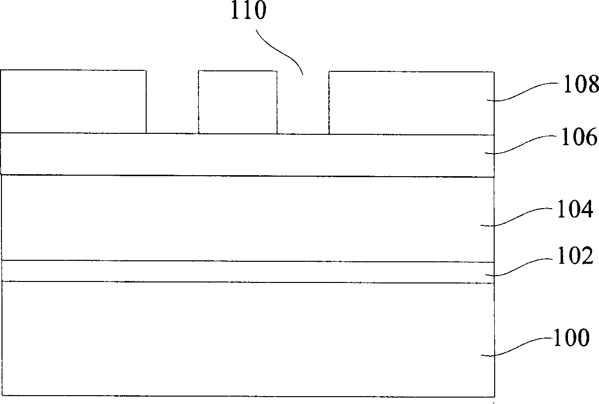
[0032] Such as Figure 6 As shown, firstly, a semiconductor substrate is provided, and a metal wire layer is formed in the semiconductor substrate ( S100 ). The semiconductor substrate can be polycrystalline silicon, monocrystalline silicon, amorphous silicon, silicon-on-insulator (SOI), gallium arsenide, silicon-germanium compound, etc., and the metal wire layer material can be copper, aluminum, titanium, nitride One or a combination of titanium and tungsten, the metal wire layer in this embodiment is copper.

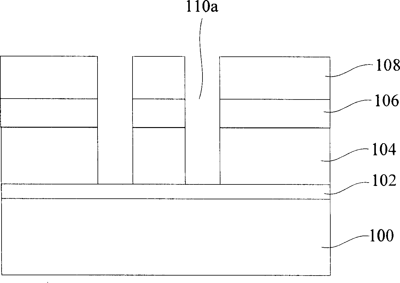
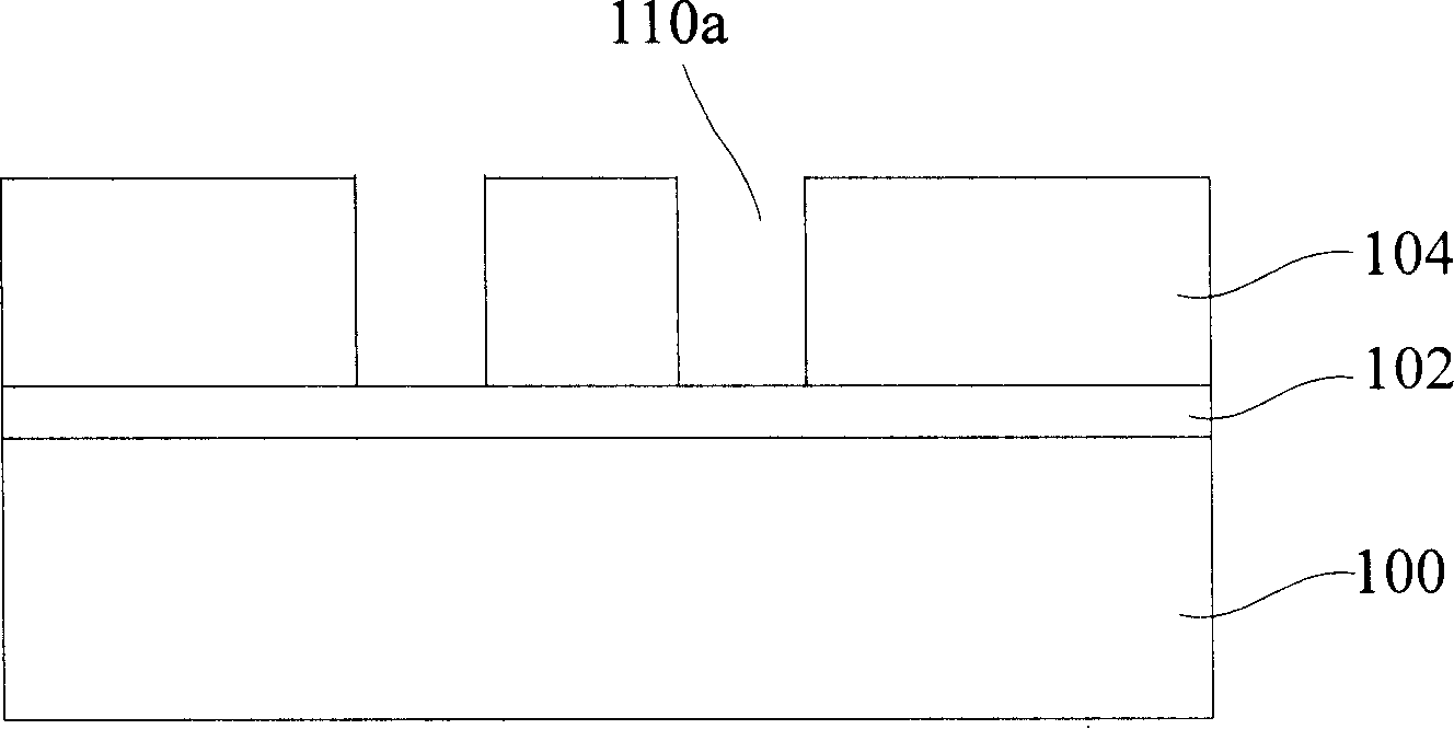
[0033] An etching stop layer is formed on the semiconductor substrate, a dielectr...


PUM


Abstract

The invention relates to a manufacturing method of a mosaic structure. The method comprises the following steps: a semiconductor substrate with a metal conducting wire layer is provided; a dielectric layer is formed on the semiconductor substrate, an opening is formed in the dielectric layer, and the bottom part of the openingis exposed outside the surface of the metal conducting wire layer; first metal layers are deposited at the bottom part and on the side wall of the opening; the first metal layer at the bottom part of the opening is removed, and the oxide on the surface of the metal conducting wire layer at the bottom part of the opening is removed; second metal layers are deposited at the bottom part and on the side wall of the opening; third metal layers are deposited on the second metal layers. The method can eliminate the coupling current which is generated by the plasma in the metal conducting wire layer, and reduce or eliminate the damage to the gate oxide.

Description

technical field [0001] The invention relates to the technical field of semiconductor manufacturing, in particular to a method for manufacturing a damascene structure. Background technique [0002] As the line width of the semiconductor process decreases day by day, the industry chooses copper instead of aluminum as the back-end interconnection material, and correspondingly chooses low dielectric constant material as the insulating material. Since copper is difficult to etch and easy to diffuse, the industry introduces the damascene process. , overcome the disadvantage of being difficult to etch, and introduce a barrier layer to block the diffusion of copper in low dielectric constant materials. The Chinese patent application number 02106882.8 discloses a mosaic process, Figure 1 to Figure 4 It is a schematic cross-sectional view of the manufacturing method of the disclosed damascene process. [0003] Such as figure 1 As shown, a substrate 100 having a metal wire layer is...

Claims


Application Information

Patent Timeline
IPC IPC(8): H01L21/768H01L23/522
Inventor 聂佳相杨瑞鹏康芸
Owner SEMICON MFG INT (SHANGHAI) CORP
Why Eureka
Try Eureka