

Metamaterial microstrip line based radiation-proof mobile phone enclosure
A technology of anisotropic medium and microstrip line, which is applied in the direction of telephone structure, electrical components, magnetic field/electric field shielding, etc., can solve the problems of reducing antenna human body radiation, poor practicability, and limited application range, etc.
- Summary
- Abstract
- Description
- Claims
- Application Information
AI Technical Summary
Problems solved by technology
Method used
Image

Examples
Embodiment 1
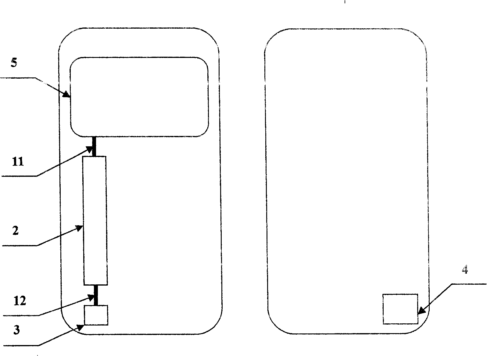
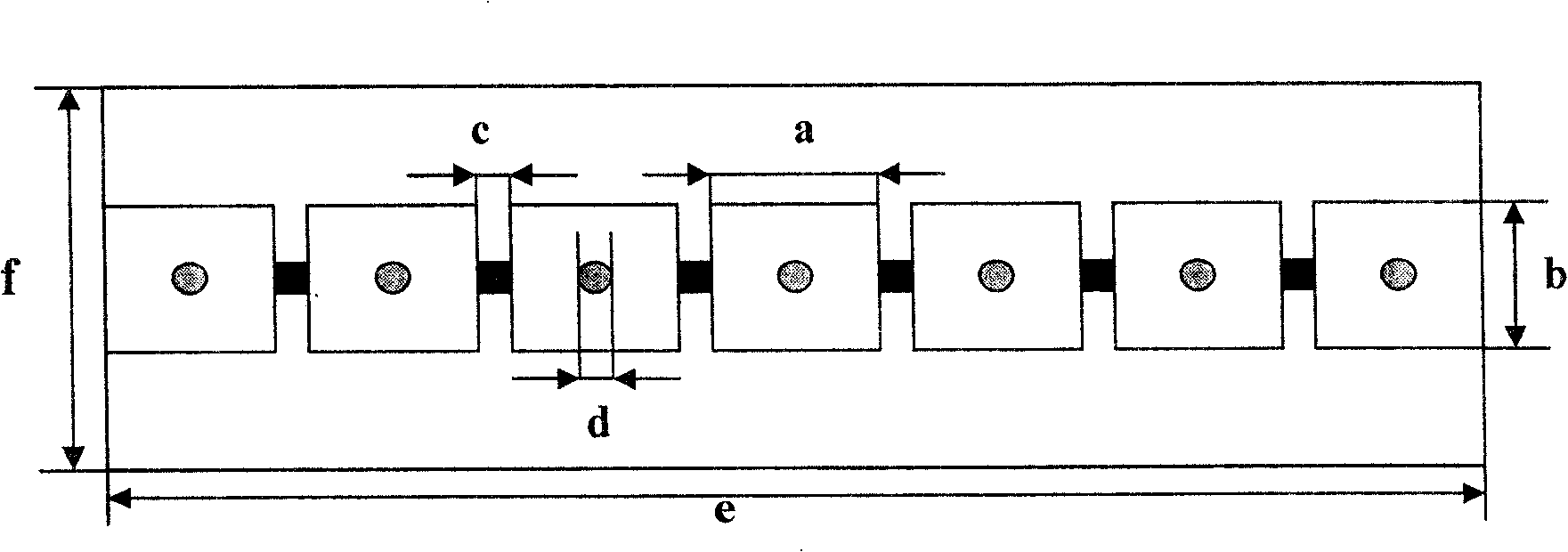
[0021] Using circuit board etching technology to make anisotropic dielectric microstrip line substrate, choose epoxy phenolic resin copper-clad dielectric board, its dielectric constant is = 4.65, board length e = 34.238mm, width f = 7mm, and the thickness of the dielectric substrate is 1.5 mm, the thickness of double-sided copper clad is 0.018mm. Select one side of the substrate as the ground plane, and etch 7 rectangular metal pieces of equal size on the other side along the center line, the length of each metal piece is a=4.238mm, the width b=2.8mm, and the width of the gap between the pieces is c = 0.762 mm. Solder 6 chip capacitors with C=2.0pF in the center of the gap between adjacent metal sheets in sequence, and the two ends are respectively connected to the adjacent metal sheets. And drill a through hole with d=1.2mm in the center of each metal sheet, and then insert a chip inductor of L=1.0nH into each through hole, weld the upper end with the metal sheet, and conne...
Embodiment 2
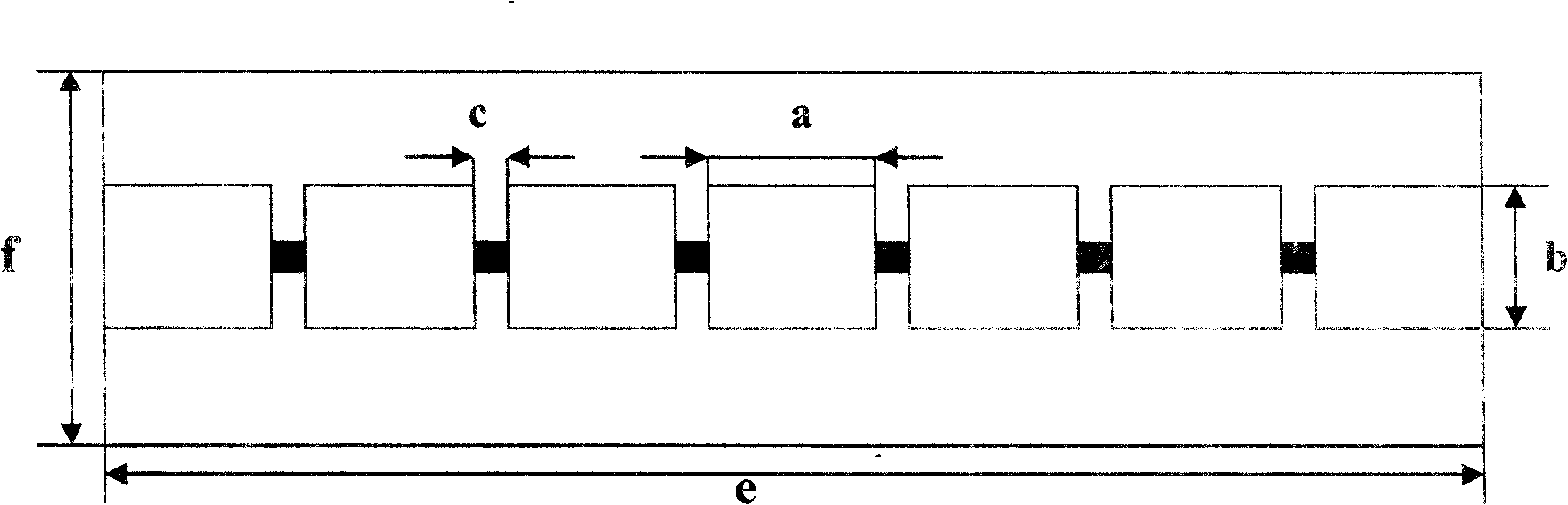
[0023] Using circuit board etching technology to make anisotropic dielectric microstrip line substrate, choose epoxy phenolic resin copper-clad dielectric board, its dielectric constant is = 4.65, board length e = 34.238mm, width f = 7mm, and the thickness of the dielectric substrate is 1.5 mm, the thickness of double-sided copper clad is 0.018mm. Select one side of the substrate as the ground plane, and etch 7 rectangular metal pieces of equal size on the other side along the center line, the length of each metal piece is a=4.238mm, the width b=2.8mm, and the width of the gap between the pieces is c = 0.762 mm. Weld 6 chip capacitors with C=1.0pF in the center of the gap between adjacent metal sheets in turn, and the two ends are respectively connected to the adjacent metal sheets. In this way, a new type of microstrip transmission line with negative magnetic permeability is produced. image 3 shown. After testing, the S21 transmission curve of the microstrip line is as at...
Embodiment 3
[0025] Using circuit board etching technology to make anisotropic dielectric microstrip line substrate, choose epoxy phenolic resin copper-clad dielectric board, its dielectric constant is = 4.65, board length e = 34.238mm, width f = 7mm, and the thickness of the dielectric substrate is 1.5 mm, the thickness of double-sided copper clad is 0.018mm. Select one side of the substrate as the ground plane, and etch 7 rectangular metal pieces of equal size on the other side along the center line, the length of each metal piece is a=4.238mm, the width b=2.8mm, and the width of the gap between the pieces is c = 0.762 mm. Drill a through hole of d=1.2mm in the center of each section of metal sheet, and then insert a chip inductor of L=1.0nH into each through hole, weld the upper end with the metal sheet, and connect the lower end with the ground plate .In this way, a new type of negative dielectric constant microstrip transmission line is produced. Figure 4 shown. After testing, the...
PUM
| Property | Measurement | Unit |
|---|---|---|
| Thickness | aaaaa | aaaaa |
| Width | aaaaa | aaaaa |
| Length | aaaaa | aaaaa |
Abstract
Description
Claims
Application Information