Package, subassembly and methods of manufacturing thereof

A technology of sub-assemblies and subassemblies, applied in semiconductor/solid-state device manufacturing, semiconductor/solid-state device components, electrical components, etc., can solve the problems of reducing substrates, easy to break, fragile silicon substrates, etc., to reduce assembly costs and complexity, The effect of reducing thickness

Inactive Publication Date: 2008-07-02
KONINKLIJKE PHILIPS ELECTRONICS NV
View PDF1 Cites 14 Cited by
  • Summary
  • Abstract
  • Description
  • Claims
  • Application Information

AI Technical Summary

Problems solved by technology

[0007] However, the known device has the disadvantage that a thickness of less than 250 microns is required for proper heat transfer through the interconnection elements on the basis of a silicon substrate
At the same time, silicon substrates of this thickness tend to be very fragile and prone to breakage
If the thickness of the substrate is further reduced, the silicon may become flexible, but the interconnection elements are no longer suitable as supporting elements for the assembly

Method used


Image

  • Package, subassembly and methods of manufacturing thereof
  • Package, subassembly and methods of manufacturing thereof
  • Package, subassembly and methods of manufacturing thereof

Examples


Embodiment Construction

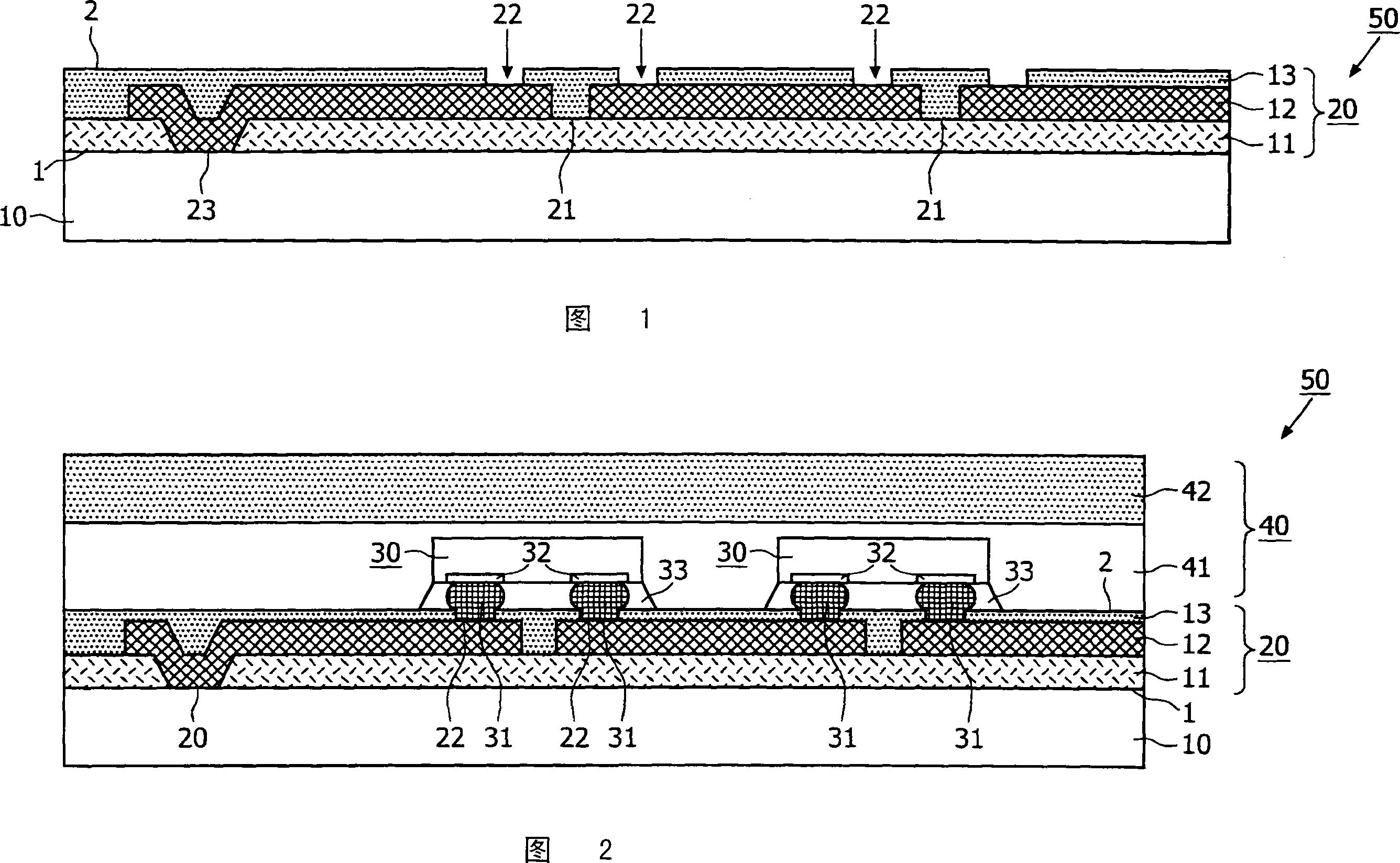
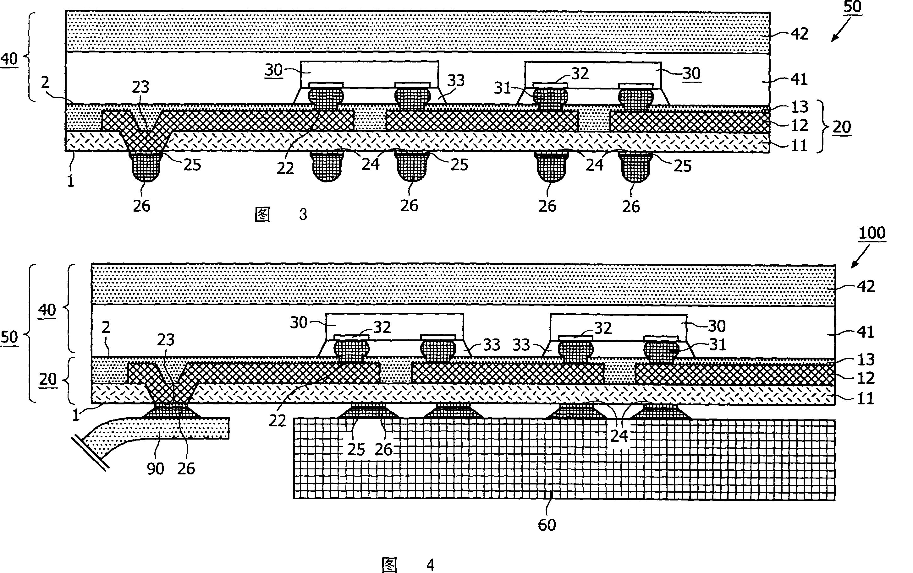
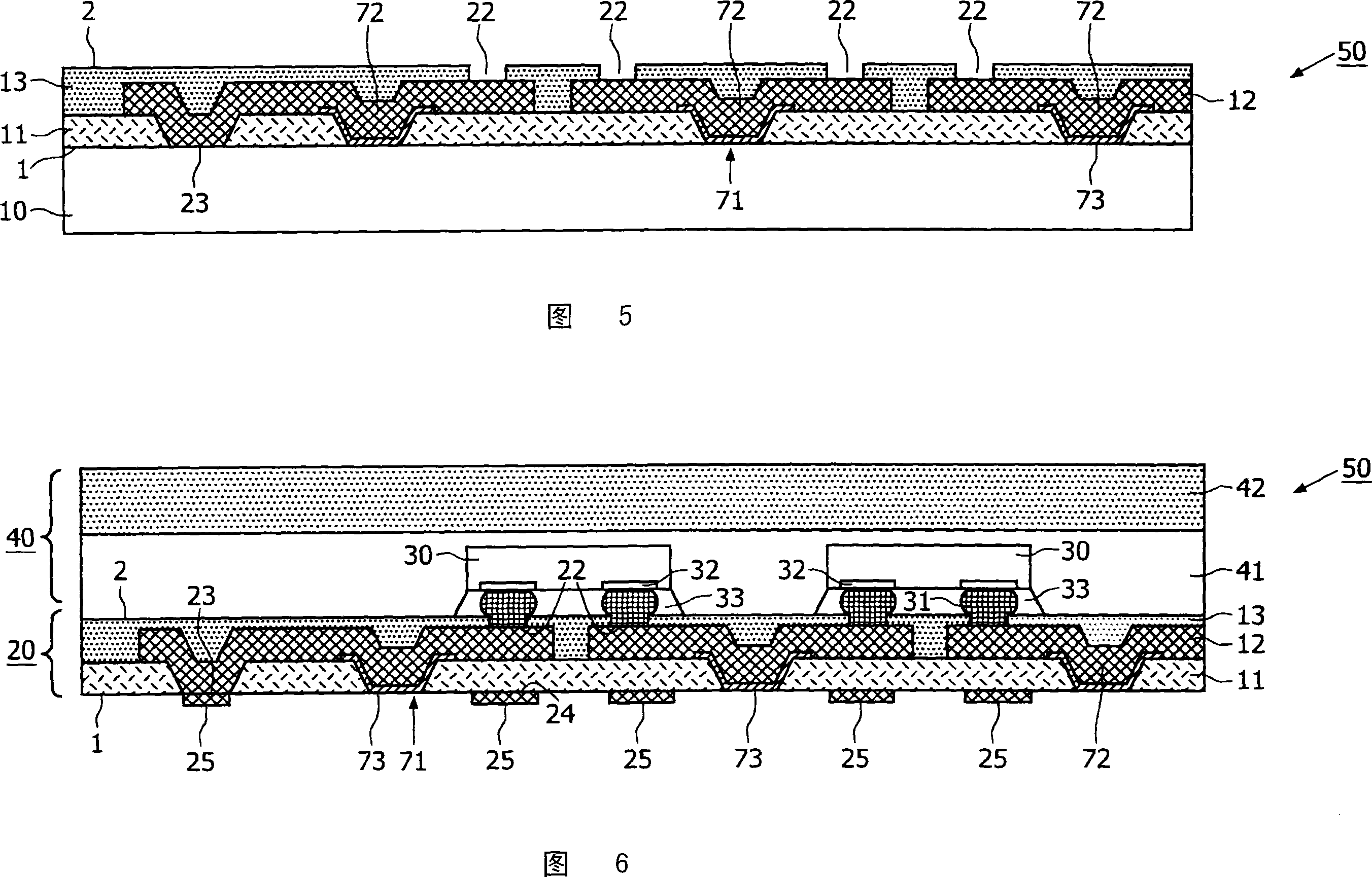
[0028] The drawings are not drawn to scale and are schematic only. The same reference numerals in different figures relate to equal or corresponding parts. The drawings are drawn for purposes of illustration only and are not to be construed as limiting the invention. Indeed, many more examples will be apparent to those skilled in the art based on the description of these figures. Although these figures show only a few stages in the fabrication of a single device, it has been found that these steps in the process generally occur at the plate level, after which breakup into individual elements occurs. This splitting can be accomplished using conventional techniques. It is appropriate that the splitting channels have been specifically defined in the subassembly 50, 150 during the manufacturing process.

[0029]FIG. 1 shows a cross-sectional view of a first stage in the manufacture of a subassembly 50 including a package but not including a heat sink. The subassembly 50 at thi...


PUM


Abstract

The package (100) of the invention comprises at least one semiconductor device (30) provided with bond pads (32); an encapsulation (40), an interconnect element (20) and a heatsink (90). This element comprises a system of electrical interconnects (12) and is at least substantially covered by a thermally conductive, electrically insulating layer (11) at a first side (1) and that is provided with an electric isolation (13) at a second side (2), such that the isolation (13) and the thermally conducting layer (11) electrically isolate the electrical interconnects (12) from each other. At least one component of the encapsulation (40) and the heatsink (90) has an interface with the interconnect element (20), which interlace extends over substantially the complete side (1,2) to which the said component (40,90) is attached.

Description

technical field [0001] The invention relates to an assembly for at least one semiconductor device, such an assembly comprising: [0002] at least one semiconductor device provided with bond pads, and [0003] an interconnection element with a first side and an opposite second side, the element comprising an electrical interconnection system at least substantially covered by a thermally conductive layer on the first side and provided with electrical isolation on the second side, This electrical isolation is provided with holes exposing contact pads defined in the interconnections to which the bonding pads of the at least one semiconductor device are electrically coupled, the interconnection element being provided with at least one terminal. [0004] The invention also relates to subassemblies of such assemblies. [0005] The invention also relates to methods of manufacturing such subassemblies and to methods of manufacturing such assemblies. Background technique [0006] S...

Claims


Application Information

Patent Timeline
Patent Type & Authority Applications(China)
IPC IPC(8): H01L23/36H01L21/68H01L21/48H01L33/62H01L33/64
CPCH01L21/486H01L21/4882H01L21/6835H01L23/36H01L23/3677H01L23/3735H01L25/0753H01L33/62H01L33/641H01L2224/05571H01L2224/05573H01L2224/16H01L2224/73204H01L2924/00014H01L2924/01078H01L2924/09701H01L2924/15311H01L2224/05599
Inventor R·德克T·M·米切尔森E·J·梅杰
Owner KONINKLIJKE PHILIPS ELECTRONICS NV
Why Eureka
Try Eureka