Solid imaging element and manufacturing method thereof

A technology of image sensor and manufacturing method, which is applied in the direction of semiconductor devices, image communication, electric solid devices, etc., can solve the problems of small opening area, poor chip usage efficiency, increased cost of area, etc., and achieve the effect of improving optoelectronics

Inactive Publication Date: 2008-07-23
SONY CORP
View PDF0 Cites 68 Cited by
  • Summary
  • Abstract
  • Description
  • Claims
  • Application Information

AI Technical Summary

Problems solved by technology

[0014] However, since the CMOS image sensor of the structure shown in FIG. 52 has a photodiode PD-sensor circuit area 32 and an ADC-storage area 33 in one semiconductor chip, when the number of pixels is increased and the res

Method used


Image

  • Solid imaging element and manufacturing method thereof
  • Solid imaging element and manufacturing method thereof
  • Solid imaging element and manufacturing method thereof

Examples


Example Embodiment

[0089] Embodiments of the present invention will be described below with reference to the accompanying drawings.

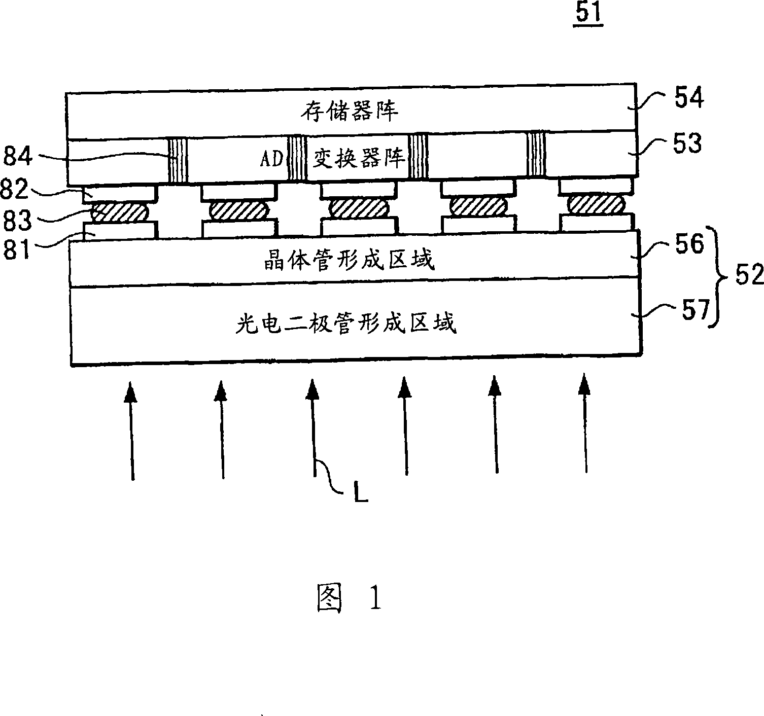
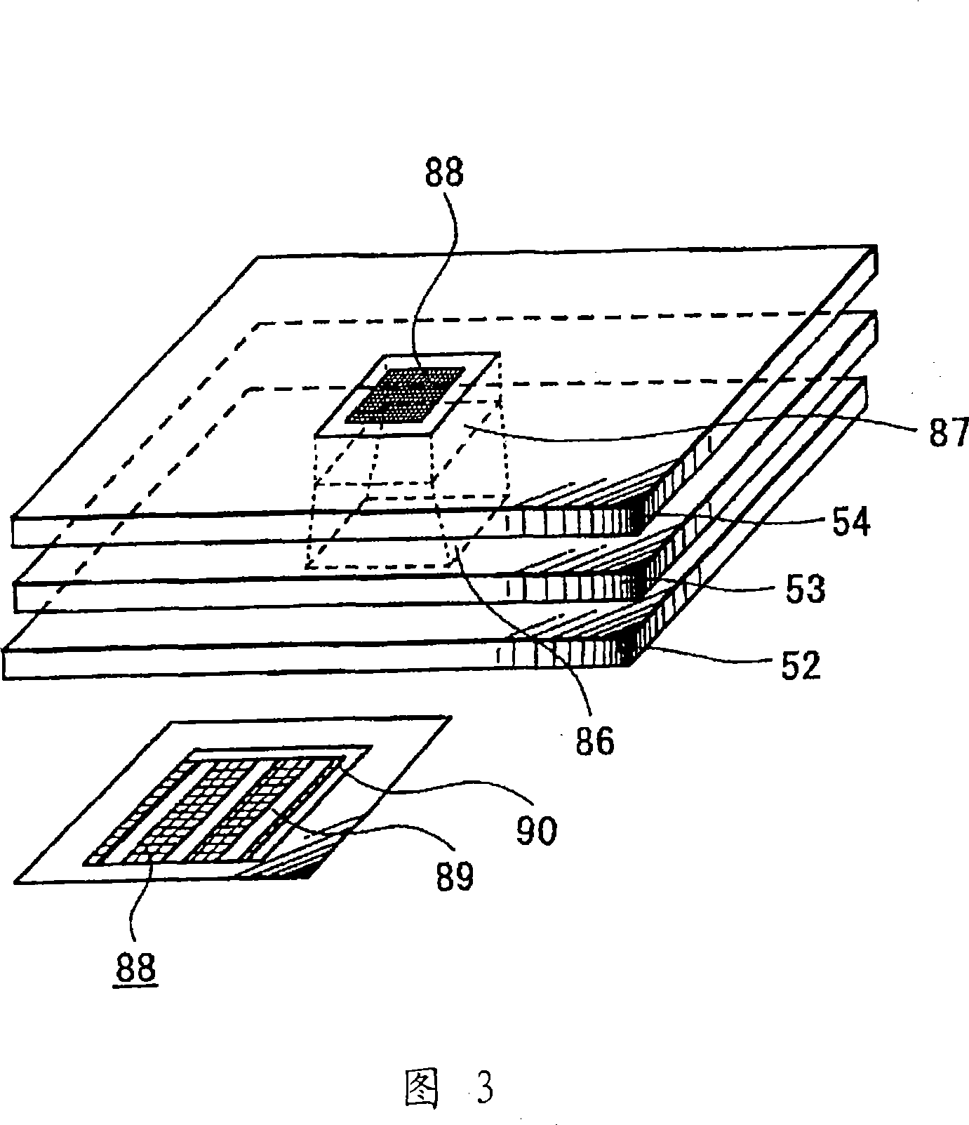
[0090] FIG. 1 shows a schematic configuration of a first embodiment of a semiconductor image sensor module of the present invention. The semiconductor image sensor module 51 according to the embodiment of the present invention is laminated with: a first semiconductor chip 52 including an image sensor in which a plurality of pixels are regularly arranged and each pixel is composed of a photodiode and a transistor serving as a photoelectric conversion element; a second semiconductor chip 53, which includes an analog-to-digital converter array (so-called analog-to-digital conversion circuit) composed of a plurality of analog-to-digital converters; and a third semiconductor chip 54, which includes a memory element array including at least an encoder and a sense amplifier .

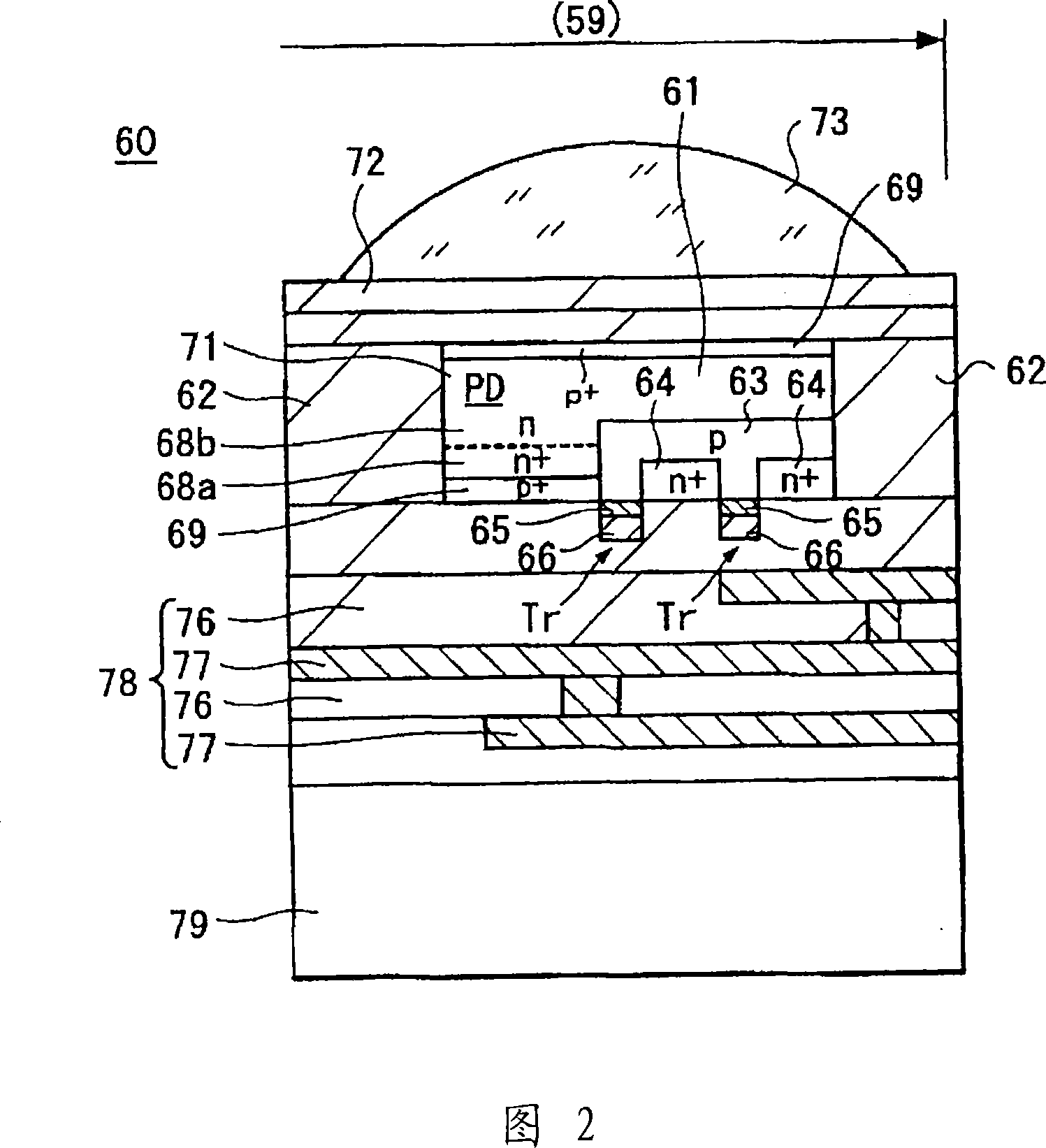
[0091] In the image sensor of the first semiconductor chip 52, in this example, a transistor ...


PUM


Abstract

A CMOS type semiconductor image sensor module wherein a pixel aperture ratio is improved, chip use efficiency is improved and furthermore, simultaneous shutter operation by all the pixels is made possible, and a method for manufacturing such semiconductor image sensor module are provided. The semiconductor image sensor module is provided by stacking a first semiconductor chip, which has an image sensor wherein a plurality of pixels composed of a photoelectric conversion element and a transistor are arranged, and a second semiconductor chip, which has an A/D converter array. Preferably, the semiconductor image sensor module is provided by stacking a third semiconductor chip having a memory element array. Furthermore, the semiconductor image sensor module is provided by stacking the first semiconductor chip having the image sensor and a fourth semiconductor chip having an analog nonvolatile memory array.

Description

technical field [0001] The present invention relates to a semiconductor image sensor module and a method of manufacturing the same. More specifically, it relates to a semiconductor image sensor module that simultaneously shields light in response to increased shutter speeds such as digital still-picture cameras, video cameras, and cell phones with cameras. Background technique [0002] Compared with CCD image sensors, CMOS image sensors have the advantage of being easy to implement a system-on-chip because they can be fabricated with a single power supply, low power consumption, and can be fabricated using standard CMOS processing. In recent years, CMOS image sensors have been used in advanced single-lens reflex digital still-picture cameras and mobile phones by taking advantage of this advantage. [0003] 54 and 55 show simplified structures of a CCD image sensor and a CMOS image sensor, respectively. [0004] As shown in FIG. 54 , in the CCD image sensor 1, a plurality o...

Claims


Application Information

Patent Timeline
IPC IPC(8): H01L27/14H01L27/00H01L27/10H01L27/146H04N5/335
Inventor 岩渊信元吉真
Owner SONY CORP
Why Eureka
Try Eureka