Circuit design standard and implementation method for 3-D solid structure phase change memory chip

A phase-change memory, three-dimensional technology, applied in static memory, read-only memory, digital memory information, etc., can solve problems that are not conducive to low voltage and low power consumption of chips

Active Publication Date: 2008-08-06
SHANGHAI INST OF MICROSYSTEM & INFORMATION TECH CHINESE ACAD OF SCI
View PDF0 Cites 13 Cited by
  • Summary
  • Abstract
  • Description
  • Claims
  • Application Information

AI Technical Summary

Problems solved by technology

Strict requirements on area will inevitably lead circuit designers to give up performance in terms of speed and power consumption in exchange for area, which is not conducive to the realization of low-voltage, low-power consumption, high-speed and high-density chip design

Method used


Image

  • Circuit design standard and implementation method for 3-D solid structure phase change memory chip
  • Circuit design standard and implementation method for 3-D solid structure phase change memory chip
  • Circuit design standard and implementation method for 3-D solid structure phase change memory chip

Examples


Embodiment Construction

[0027] For further clarifying substantive characteristics of the present invention and remarkable progress, describe the present invention by embodiment below:

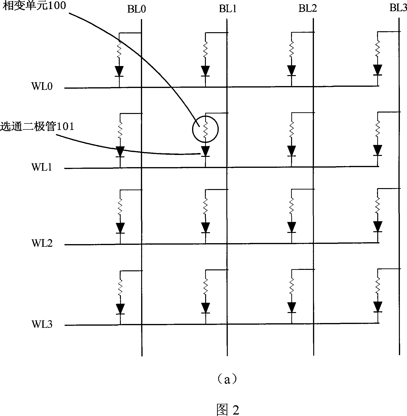
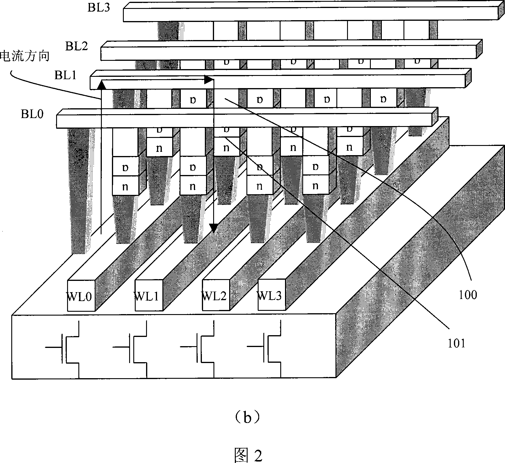
[0028]Fig. 2a is a pattern of a 4×4 array of a phase-change memory 1R1D (a diode D is connected to a phase-change memory unit R). It should be understood that the present invention is not limited thereto. 100 in the figure is a phase-change memory unit, and 101 is a gate diode. When the read / write operation is not performed on 100 , the bit line BL1 and the word line WL1 maintain a potential that can ensure that the gate diode 101 is turned off. For example, WL1 may be logic “1” and BL1 may be logic “0”; or BL1 may be in a floating state; or BL1 may be an intermediate level value. When 100 is to be read and written, WL1 is reduced to logic "0", BL1 inputs current or a certain voltage value is given, so that 101 is turned on, ensuring that a certain current value flows through the phase-change memory unit. When a cu...


PUM


Abstract

The invention relates to a circuit design criteria and a realization method for a three-dimensional structure phase transition memory chip. In order to utilize the memory area to a maximum extent, the invention requires that the whole memory chip is studded with memory arrays. The circuit structure provided is an optimization proposal aiming at the characteristic that the whole memory chip is studded with the memory arrays. The invention has the advantages that the whole memory chip can be studded with the memory arrays. In order to realize the advantage, firstly, peripheral circuits under the memory arrays are divided reasonably; secondly, a set of solution proposal is provided for mutual control problem of the peripheral circuits after division; thirdly, a splicing proposal of the peripheral circuits is provided on the basis of the first step and the second step. Therefore, the three-dimensional structure phase transition memory chip is completely realized in the aspect of circuit design.

Description

technical field [0001] The invention aims at the overall circuit design criteria and implementation method of a three-dimensional three-dimensional structure phase-change memory chip, and relates to the field of large-scale integrated circuits. Background technique [0002] Chalcogenide-Random Access Memory (C-RAM) is based on S.R.Ovshinsky in the late 1960s and early 1970s (Phys. Rev. Lett., 21, 1450-1453, 1968); (Appl. Phys. Lett., 18, 254-257, 1971) developed on the basis of the idea that the chalcogenide thin film can be applied to phase-change storage media. In 2001, Intel Corporation reported 4MB C-RAM for the first time, and Samsung Corporation reported 512MB C-RAM by the end of 2006. At present, the mainstream non-volatile memory is mainly flash memory. However, according to Moore's law, when the existing memory cell design is below 45nm, it is difficult to maintain its non-volatile characteristics. Since phase change memory does not need to erase the original dat...

Claims


Application Information

Patent Timeline
Patent Type & Authority Applications(China)
IPC IPC(8): G11C11/56G11C16/02H01L27/115
Inventor 宋志棠丁晟刘波宝民封松林刘卫丽
Owner SHANGHAI INST OF MICROSYSTEM & INFORMATION TECH CHINESE ACAD OF SCI
Why Eureka
Try Eureka