

Making method for low-temperature multi-crystal silicon film
A technology of low-temperature polysilicon and a manufacturing method, which is applied in the manufacture of semiconductor/solid-state devices, electrical components, circuits, etc., can solve the problems of uneven size of polysilicon grains, uncontrollable position of polysilicon grains, etc., and achieves large size and high performance. Uniform, performance-enhancing effect
- Summary
- Abstract
- Description
- Claims
- Application Information
AI Technical Summary
Problems solved by technology
Method used
Image

Examples
Embodiment Construction
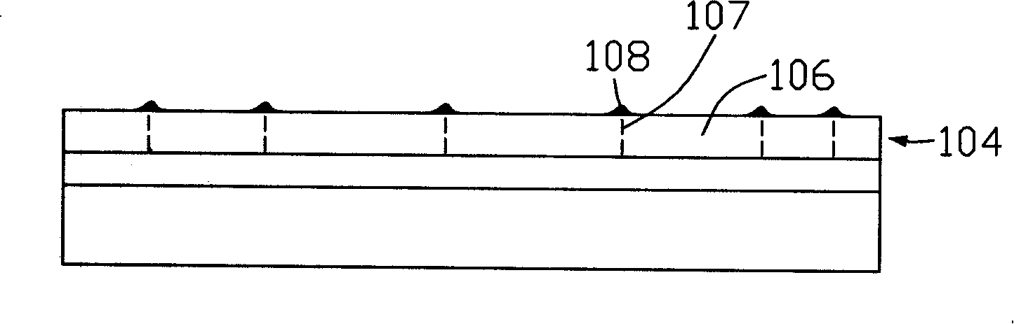
[0018] Please also refer to Figure 5 to Figure 11 , which is a schematic diagram corresponding to each step of a preferred embodiment of the method for manufacturing a low-temperature polysilicon thin film according to the present invention. The method for manufacturing a low-temperature polysilicon thin film mainly includes the following steps:
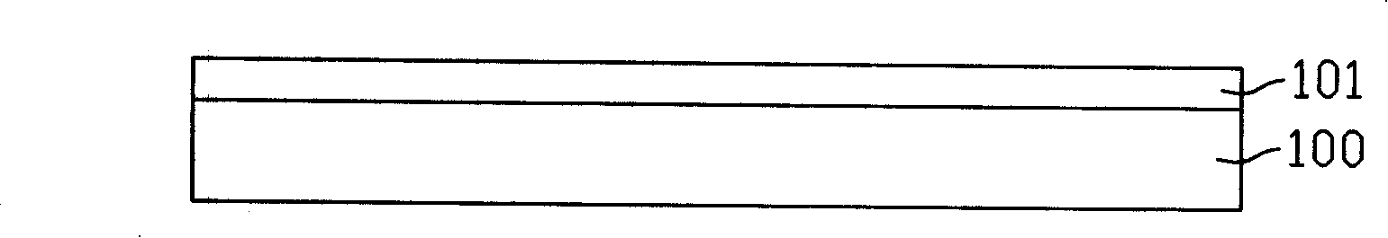
[0019] 1. Provide a substrate and form a buffer layer thereon;
[0020] see Figure 5 Firstly, a substrate 200 is provided, and the substrate 200 is a glass substrate or a plastic substrate. A buffer layer 201 is formed on the substrate 200, and the buffer layer 201 is a silicon nitride layer or a silicon oxide layer, and may also be a multi-layer structure including a silicon nitride layer and a silicon oxide layer. The buffer layer 201 is used to prevent substances in the substrate 200 from diffusing in subsequent processes and affecting the quality of the produced low temperature polysilicon thin film.
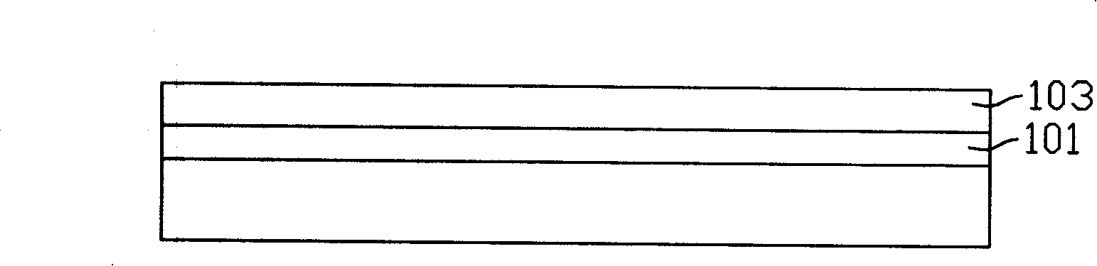
[0021] 2. Forming the ...
PUM
| Property | Measurement | Unit |
|---|---|---|
| Spacing | aaaaa | aaaaa |
Abstract
Description
Claims
Application Information