

Thin film transistor device, method of manufacturing the same, and display apparatus
A thin-film transistor, thick and thin technology, applied in the direction of transistors, electric solid-state devices, semiconductor devices, etc., can solve the problems of increased cut-off current and inability to obtain transistor characteristics, etc., to reduce leakage, reduce contact resistance, and improve The effect of pressure resistance
- Summary
- Abstract
- Description
- Claims
- Application Information
AI Technical Summary
Problems solved by technology
Method used
Image

Examples
Embodiment approach 1
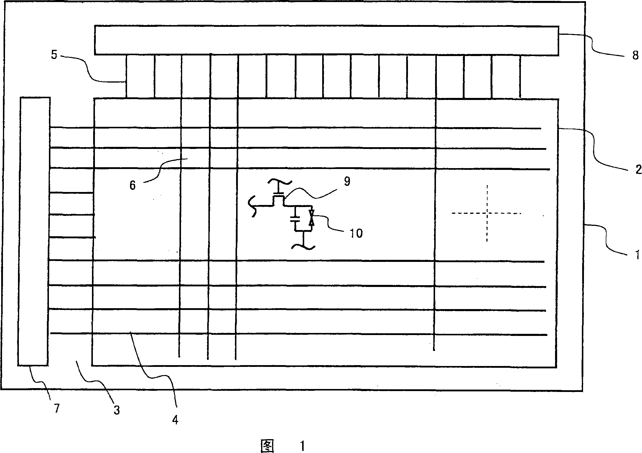
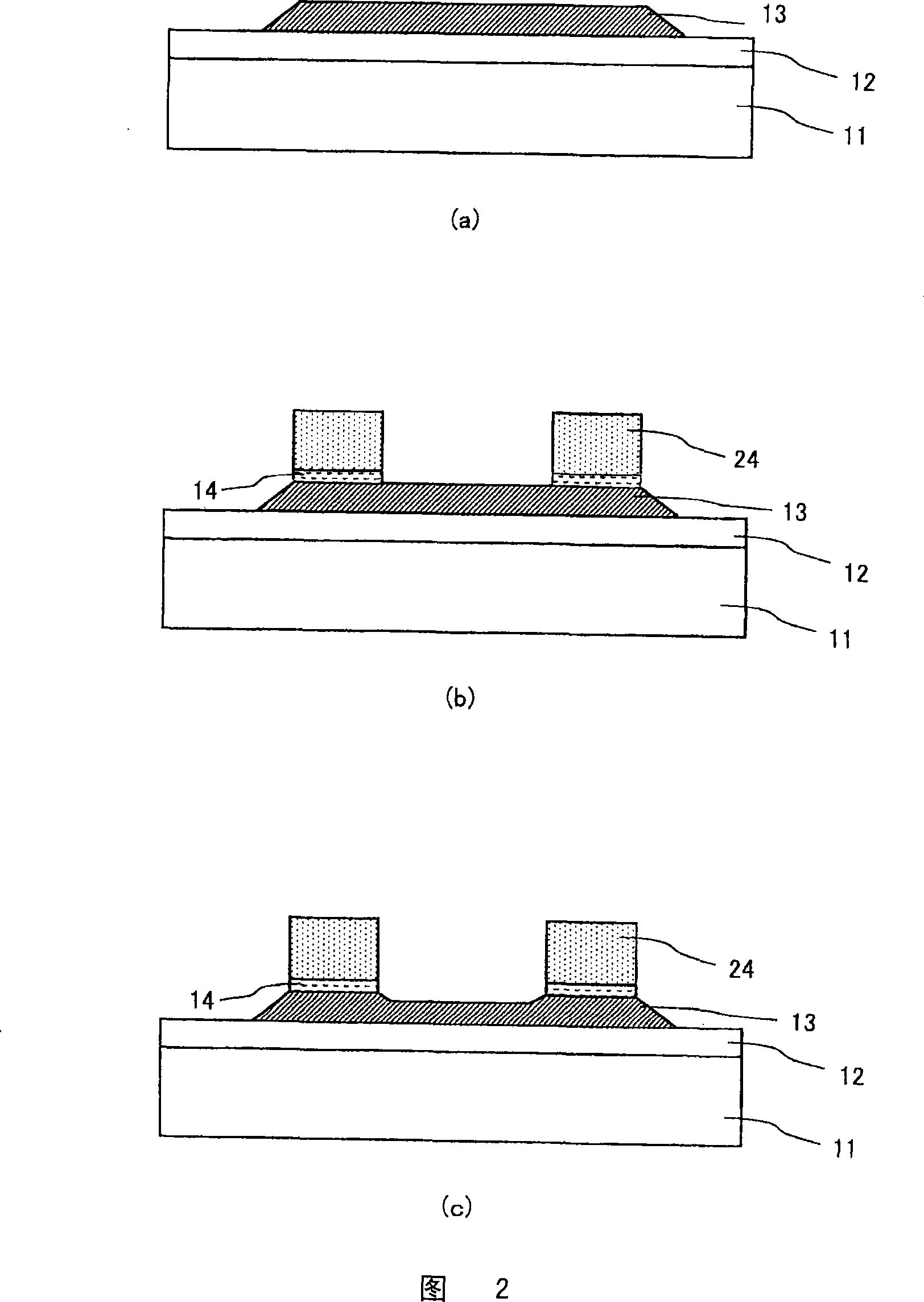
[0033] The specific implementation manners of the present invention will be described in detail below with reference to the accompanying drawings. The thin film transistor device according to the embodiment of the present invention constitutes a TFT array (TFT array) substrate 1 . FIG. 1 is a schematic plan view showing the structure of a TFT array substrate 1 of the present embodiment. The TFT array substrate 1 has a display area 2 and a frame area 3 provided to surround the display area 2 . In this display region 2, a plurality of gate signal lines 4 and a plurality of source signal lines 5 are formed. The plurality of gate signal lines 4 are respectively arranged in parallel. Likewise, a plurality of source signal lines 5 are respectively provided in parallel. In addition, the gate signal line 4 and the source signal line 5 are perpendicular to each other. A region surrounded by the gate signal line 4 and the source signal line 5 becomes a pixel 6 . That is, on the TFT...
Embodiment approach 2
[0052] A display device according to Embodiment Mode 2 will be described with reference to FIG. 7 . 7 is a cross-sectional view of a TFT device according to Embodiment 2. FIG. In the TFT device of the second embodiment shown in FIG. 7 , the same components as those of the first embodiment shown in FIGS. 2 and 3 are denoted by the same reference numerals, and detailed description thereof will be omitted.
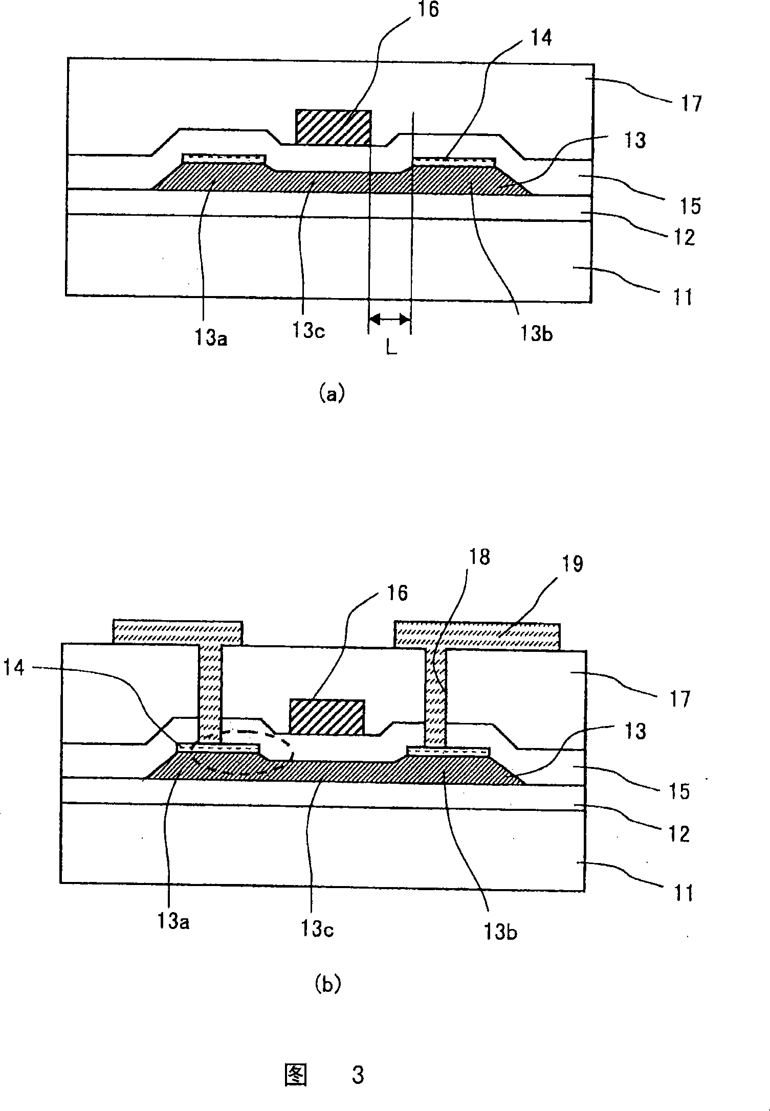
[0053] In the TFT device shown in FIG. 7, the difference from Embodiment 1 shown in FIGS. The gate insulating film 15 has a laminated film of the metal film 14 and the polysilicon film 13 on a lower electrode facing the upper electrode 20 of the storage capacitor portion.
[0054] Next, the method of manufacturing the TFT device of this embodiment will be described in detail. The detailed manufacturing method of the TFT device common to Embodiment 1 is omitted. First, when the polysilicon film 13 is patterned into an island shape and the metal film 14 is formed, the polysi...
Embodiment approach 3
[0060] A TFT device according to Embodiment 3 will be described with reference to FIG. 3( a ) and FIG. 8 . The TFT device shown in FIG. 8 differs from the TFT device of Embodiment 1 shown in FIGS. 2 and 3 in that it has an upper insulating film 21 formed on the interlayer insulating film 17; A pixel electrode 23 on the insulating film 21; an upper contact hole 22 for connecting the pixel electrode 23 and the metal film 14 is provided.
[0061] That is, in the TFT device shown in FIG. . A wiring electrode 19 connected to the source region 13 a or the drain region 13 b through the metal film 14 is formed on the interlayer insulating film 17 . The upper insulating film 21 is formed by, for example, a silicon oxide film, a silicon nitride film, or the like by CVD. Alternatively, a resin film or the like may be applied. Furthermore, a laminated film of these films may also be used. Thereafter, the upper insulating film 21 , the interlayer insulating film 17 , and the gate insu...
PUM
 Abstract
Description
Claims
Application Information