
Conductive structure for semiconductor integrated circuit and method for forming the same

A conductive structure and integrated circuit technology, which is applied in semiconductor devices, semiconductor/solid-state device manufacturing, semiconductor/solid-state device components, etc., can solve the problems of increased equivalent resistance, lower bump plating yield, and affecting plating effects, etc.

Active Publication Date: 2008-08-20
CHIPMOS TECH INC
View PDF0 Cites 0 Cited by
  • Summary
  • Abstract
  • Description
  • Claims
  • Application Information

AI Technical Summary

Problems solved by technology

However, the equivalent resistance of the underlying metal with increased thickness will increase, and since the main function of the underlying metal is to serve as an adhesive layer between bumps and pads, its impedance itself is relatively high. Therefore, if the underlying metal as an adhesive layer has a thicker thickness , will increase the impedance between the bump and the pad, which is not conducive to the electrical connection between the chip and the circuit board
All of the above situations will affect the electroplating effect, reduce the yield rate of bump electroplating, and require post-processing reformation or scrap the chip

Method used


Image

  • Conductive structure for semiconductor integrated circuit and method for forming the same
  • Conductive structure for semiconductor integrated circuit and method for forming the same
  • Conductive structure for semiconductor integrated circuit and method for forming the same

Examples


Embodiment Construction

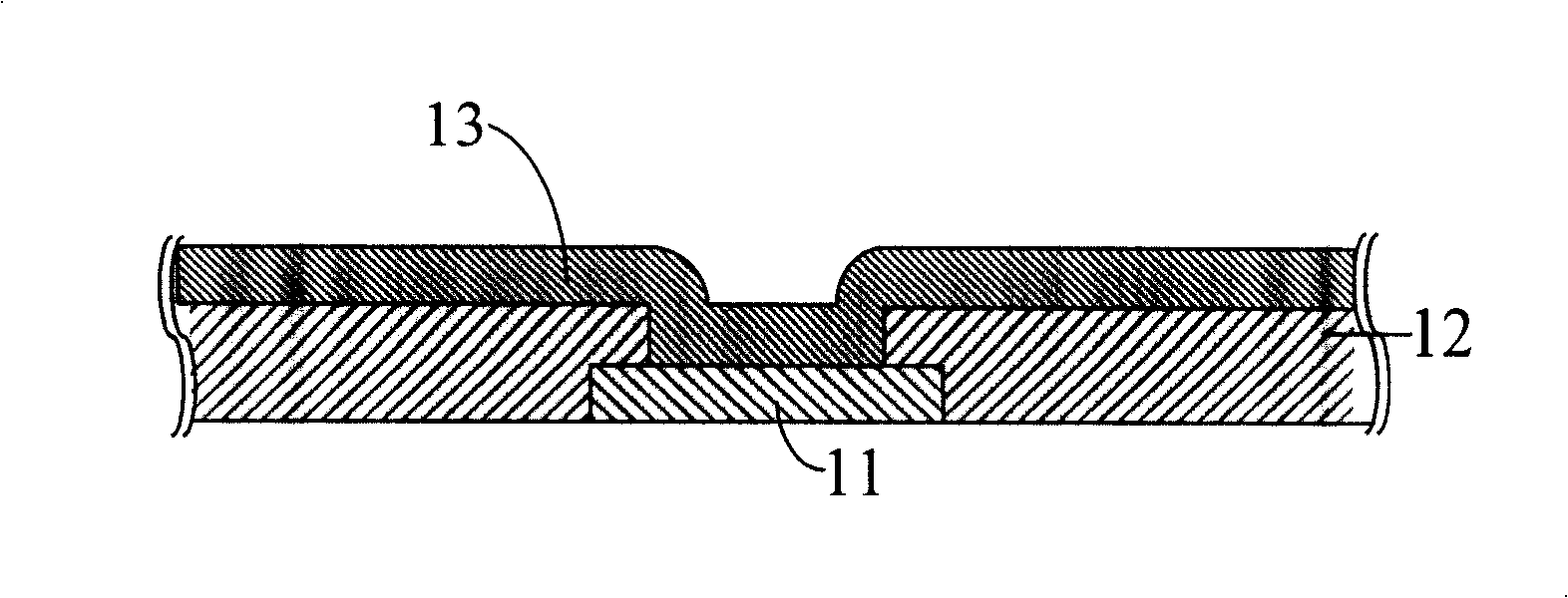
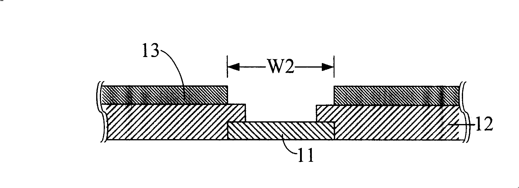
[0012] Figure 1(a) to Figure 1(h) A preferred embodiment of the present invention is shown, which is a schematic flow chart of the formation of a conductive structure for a semiconductor integrated circuit.

[0013] FIG. 1( a ) shows the initial manufacturing process, which firstly forms a liner 11 and a protective layer 12 . In this embodiment, the liner 11 is made of aluminum, and the protective layer 12 partially covers the liner 11, so that the liner 11 is exposed to define a first opening area, which is used as an electrical contact with a bump later. The connection window, wherein the first opening area has a first lateral dimension W1. Since the protective layer 12 covers the edge of the pad 11, the first opening area is smaller than the lateral dimension of the pad.

[0014] Then form a first conductive layer, such as a titanium-tungsten alloy conductive layer 13, which covers the first opening area and extends on the protective layer 12 when it is formed; as shown i...


PUM


Abstract

The invention relates to a conductive structure for a semiconductor integrated circuit and the forming method thereof. The semiconductor integrated circuit comprises a liner and a protecting layer, the liner is locally covered to define a first opening region having a first horizontal size, so that the conductive structure is capable of getting through the first opening region to electrically connect with the liner. The conductive structure covers the first opening region and partial protecting layer to provide low-resistance conductive property between the liner and a bump, at the same time, the conductive structure locates on the protecting layer in other positions with no break points being formed, and provides more stable conductivity.

Description

technical field [0001] The present invention is a conductive structure; in particular, a conductive structure for a semiconductor integrated circuit and its forming method. Background technique [0002] Bump plating has developed many technologies in the fields of microelectronics and microsystems, such as the connection between flat panel displays (FPD) and driver ICs, and the conduction on gallium arsenide chips. The bump electroplating technology is used at different stages in the wire and air bridge technology, and in the manufacture of the X-ray mask in the LIGA technology. [0003] Taking the connection between the circuit board and the IC chip as an example, the IC chip can be connected to the circuit board in various ways, and its packaging method is mainly to use bump (especially gold bump) electroplating technology to place the pads in the IC chip Electrically connected with the circuit board. This technology can not only greatly reduce the size of the IC chip, b...

Claims


Application Information

Patent Timeline
Patent Type & Authority Applications(China)
IPC IPC(8): H01L23/485H01L23/50H01L21/60
CPCH01L24/11H01L2224/11H01L2924/14H01L2924/00H01L2924/00012
Inventor 齐中邦
Owner CHIPMOS TECH INC
Learn More