Microelectrode array chip for cell electrofusion

A technology of microelectrode array and electrode array, which is applied in the direction of hybrid cell preparation, stress-stimulated microbial growth method, biochemical equipment and method, etc., can solve the problems of unfavorable sample liquid entry and exit and later cultivation, weak electric field strength and electric field gradient, Anti-corrosion, weak anti-oxidation ability and other problems, to achieve the effect of improving the internal electric field distribution, reducing physical damage, and ensuring biocompatibility

Inactive Publication Date: 2008-08-27
CHONGQING UNIV
View PDF3 Cites 13 Cited by
  • Summary
  • Abstract
  • Description
  • Claims
  • Application Information

AI Technical Summary

Problems solved by technology

Its advantage is that the number of integrated electrodes is large, and a large number of cells can be fused to a certain extent, but its disadvantage is that the flow channel is narrow, which is not conducive to the entry and exit of sample liquid and

Method used


Image

  • Microelectrode array chip for cell electrofusion
  • Microelectrode array chip for cell electrofusion
  • Microelectrode array chip for cell electrofusion

Examples


Embodiment 1

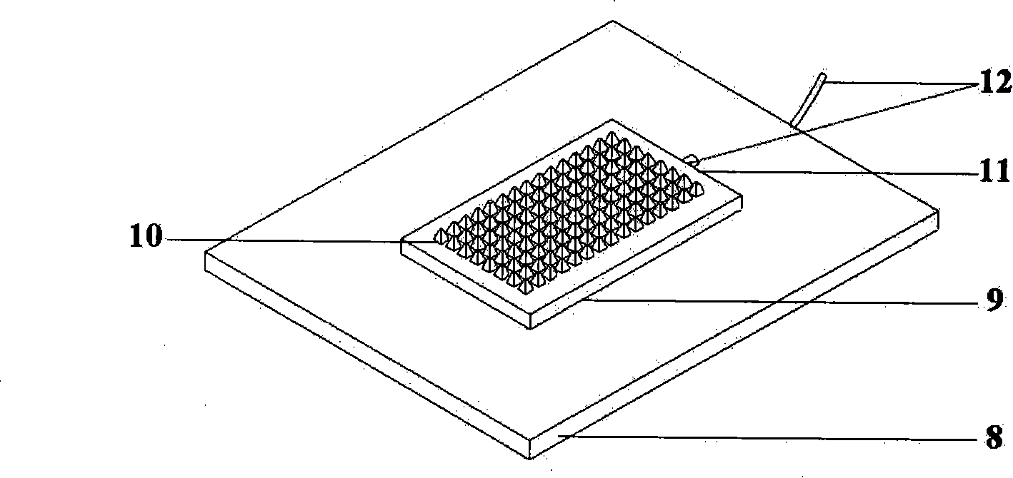
[0031] First, bond a layer of silicon wafer material on the surface of hard insulating chip processing materials such as glass, and use MEMS processing technology to etch grooves with a certain depth on the silicon wafer to form a silicon microelectrode array, and deposit platinum on the electrode surface Inert metal materials such as metals improve corrosion resistance and biocompatibility, and connect the microelectrode array with peripheral circuits through metal leads to introduce electrical signals. The fusion cell containing the sample solution is formed by etching a rectangular groove for hard conductive chips such as metals. In the experiment, the microelectrode array is immersed in the sample solution,

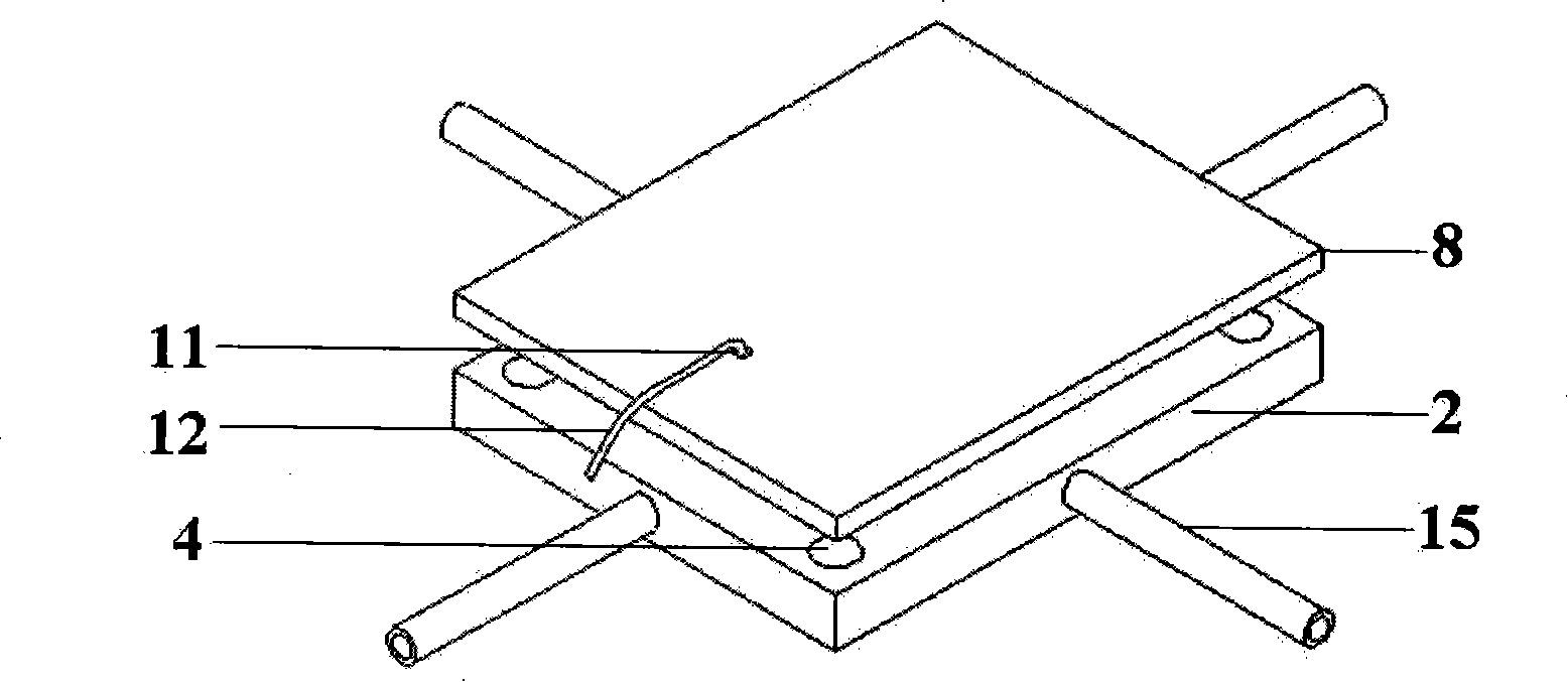
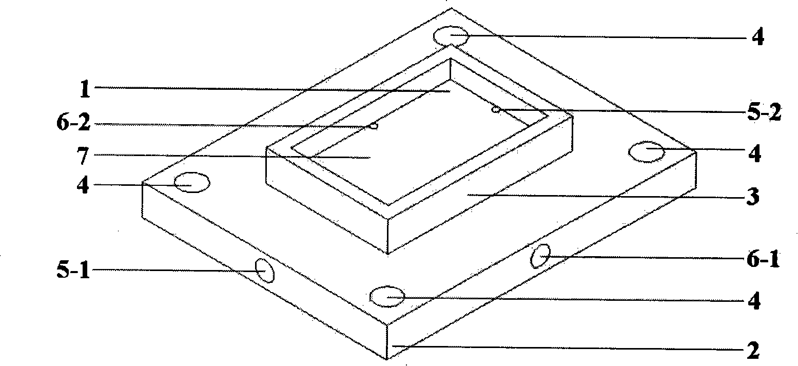
[0032] see figure 1 , the microelectrode array chip is composed of two mutually independent modules, namely the microelectrode array module A and the fusion pool and plate electrode module B.

[0033] see in conjunction figure 2 , the fusion cell and the flat elec...


PUM


Abstract

The invention provides a microelectrode array chip which is used to fuse cells electrically and is composed of a microelectrode array module, a fusion pool and a plate electrode module. The microelectrode array module is composed of a hard insulated basal layer and an electrode array layer, the electrode array layer introduces electrical signals through a metal wire, the fusion pool and the plate electrode module are composed of a base and the fusion pool on the base, the bottom of the fusion pool is also used as a plate electrode, the size of the electrode array layer on the microelectrode array module is smaller than the size of the fusion pool and the fusion pool on the plate electrode module, the microelectrode array module is covered on the fusion pool and the plate electrode module, the electrode array layer is dipped in sample solution of the fusion pool, and when external electric stimulation signals are implied, namely, an uneven gradient field with high strength is formed in tiny space between a microelectrode array and a plate electrode in the fusion pool, the process for electrically fusing the cells is realized. The chip can increase the efficiency for fusing the cells and the corrosion resistance of the chip, the biocompatibility of the microelectrode array chip is improved, and the safety and the cell vitality for fusing cells are guaranteed.

Description

technical field [0001] The invention relates to a chip structure for cell electric fusion. It specifically involves cell queuing in cell electrofusion experiments, cell electroporation, generation of electric field gradients and electric field strengths for cell electrofusion, sample injection and sample output for cell electrofusion experiments. Background technique [0002] Biological cells can form new cells through fusion, which is of great significance in the basic field of modern biomedical engineering. Cell fusion includes chemical fusion methods (such as PEG) and physical fusion methods. Among the physical fusion methods, the electric field fusion method has been widely used because of its advantages of easy precise control, good repeatability, and high fusion rate. [0003] When biological cells are in a non-uniform electric field, they are excited by the electric field to form dipoles, and the dipoles move under the force of the non-uniform electric field, that is...

Claims


Application Information

Patent Timeline
IPC IPC(8): C12M1/42C12N15/02
CPCC12M35/02C12M23/12C12M23/20
Inventor 杨军胡宁郑小林侯文生阴正勤霍丹群侯长军曹毅杨静许蓉夏斌张瑞强
Owner CHONGQING UNIV
Why Eureka
Try Eureka