Wave decomposing multiplexer based on two-dimension photon crystal

A two-dimensional photonic crystal and demultiplexer technology, which is applied in the field of optical fiber communication systems and networks, can solve the problems of system interference signals, harshness, and difficulty in device fabrication, and achieves low crosstalk between wavelength channels and high wavelength decomposition multiplexing efficiency. , the effect of improving the efficiency of WDM

Inactive Publication Date: 2011-02-09
SHANGHAI JIAOTONG UNIV
View PDF0 Cites 2 Cited by
  • Summary
  • Abstract
  • Description
  • Claims
  • Application Information

AI Technical Summary

Problems solved by technology

However, this system has a relatively harsh and complex resonance design, that is, the two microcavity modes between the two waveguides must be completely degenerate, which may bring great difficulties to device fabrication.
There is also a structural disadvantage of the four-port system, that is, it is not easy to design a multi-wavelength wavelength division multiplexer
But there is a serious problem with this device. In the reflected optical signal, except for the wavelength optical signal to be dropped into the drop waveguide, all other wavelengths of light will be reflected to the incident end
If this device is used in a large-scale integrated optical circuit, it will bring serious interference signals to the entire system
Moreover, in this design, the choice of the distance between the reflective surface and the drop waveguide has wavelength selectivity, so it is not possible to perform wave division multiplexing at any number of wavelength positions.

Method used


Image

  • Wave decomposing multiplexer based on two-dimension photon crystal
  • Wave decomposing multiplexer based on two-dimension photon crystal
  • Wave decomposing multiplexer based on two-dimension photon crystal

Examples


Embodiment

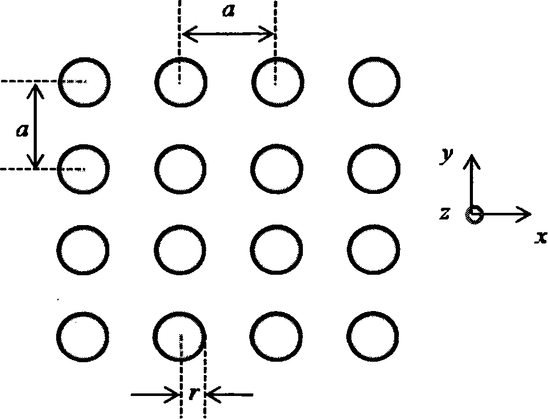
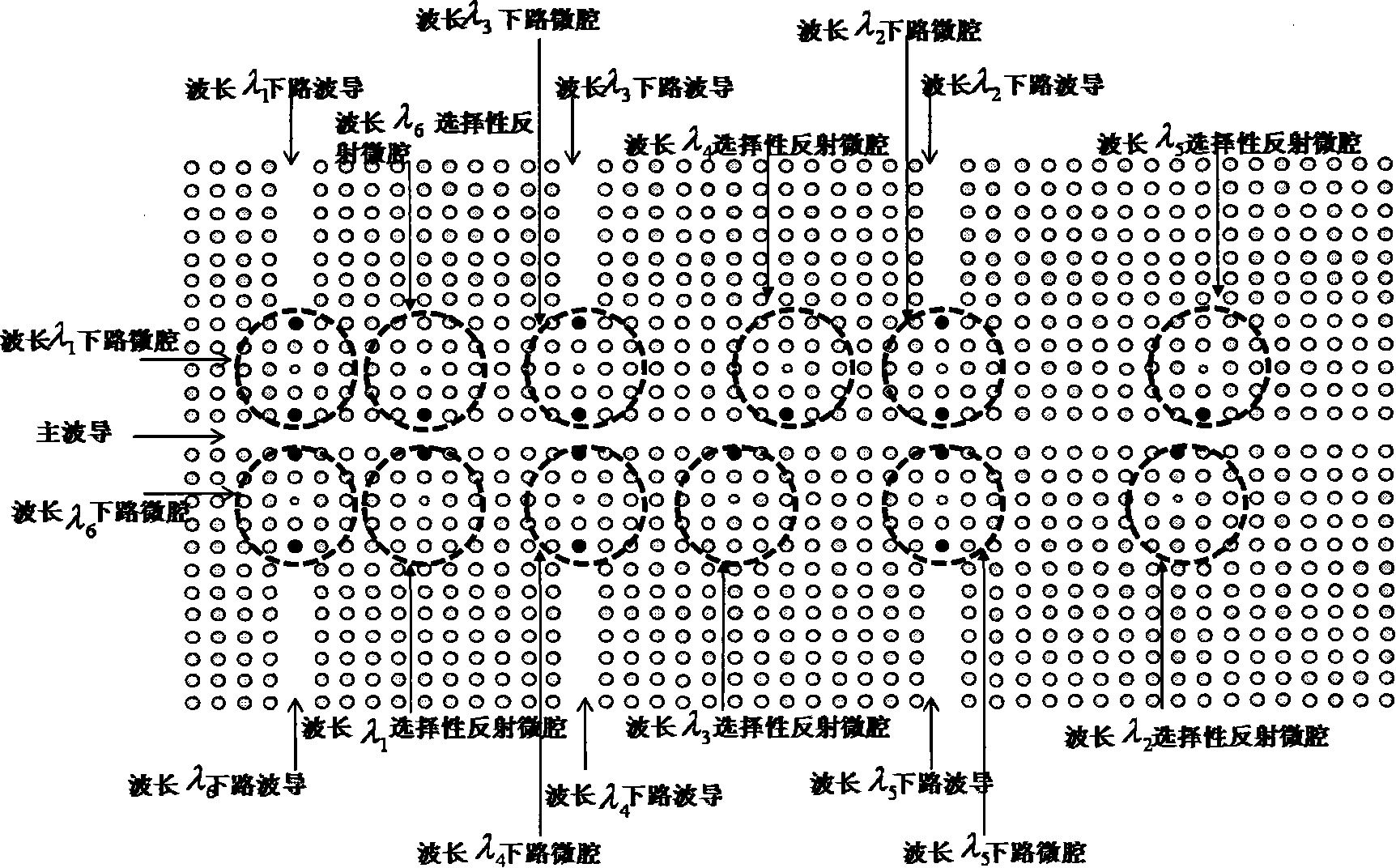
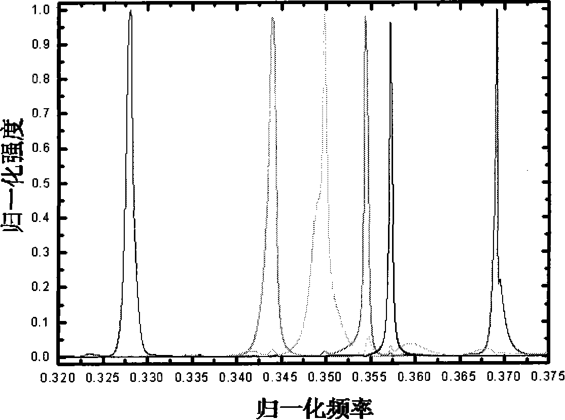
[0019] A six-wavelength wavelength division multiplexer for optical communication windows. Two-dimensional photonic crystals are composed of high-refractive-index dielectric silicon cylinders with a square lattice, and the refractive index is 3.4. The medium cylinder radius is 0.20a. Here a is the lattice constant, equal to 542nm. This kind of photonic crystal only has TM (transverse magnetic wave, electric field direction along the z direction) mode photonic bandgap with the electric field direction parallel to the dielectric column, and the normalized frequency range is 0.28688 figure 2 are represented by black circular holes. When their radii are 0.23a and 0.211a respectively, the two microcavities have the same normalized frequency of 0.36919, corresponding to a wavelength of 1550nm. Calculate the transmission spectrum of the system without wavelength selective reflection microcavity and only drop microcavity. It can be obtained that the drop efficiency of WDM in this c...


PUM


Abstract

The utility model relates to a wavelength division demultiplexer based on a two-dimensional photonic crystal, comprising a photonic crystal main waveguide, a plurality of wavelength downlink waveguides and a plurality of pairs of photonic crystal micro cavities; each pair of the photonic crystal micro cavities comprise a downlink micro cavity and a wavelength selectivity reflection micro cavity; pairs of the photonic crystal downlink micro cavities and the wavelength selectivity reflection micro cavities are respectively in staggered arrangement on both sides of the main waveguide; the photonic crystal downlink micro cavity is a point defect micro cavity used for connecting the main waveguide with the downlink waveguide; the wavelength selectivity reflection micro cavity is a point defectmicro cavity whose one side is coupled with the main waveguide; the Q factor ratio needs to fulfill a certain relation with the aim of realizing the high-efficiency wavelength division demultiplexing; meanwhile, the distance of each pair of the downlink micro cavity and the corresponding wavelength selectivity micro cavity along the main waveguide direction needs to fulfill a certain phase relation. The wavelength division demultiplexing structure has the advantages of micro size, easy integration, high-efficiency wavelength division dedmultiplexing and small cross talk; the wavelength division demultiplexer can be widely applied to the wavelength division demultiplexing optical communication system in the future.

Description

technical field [0001] The invention relates to a wave division multiplexer based on a two-dimensional photonic crystal, which is suitable for optical fiber communication systems and networks. Background technique [0002] The current optical fiber communication system widely uses wavelength division multiplexing (WDM), which can effectively use the bandwidth of optical fiber to realize large-capacity, long-distance optical fiber communication, and can increase the number of services in the user distribution system. In the application of these wavelength division multiplexing technologies, in order to make full use of very precious bandwidth resources, the wavelength channel interval becomes narrower and narrower, and the number of channels becomes more and more. This requires the size of the WDM to not only be smaller, but also easy to integrate. However, the size of the wavelength division multiplexer obtained by using the traditional silicon flat circuit or optical fiber...

Claims


Application Information

Patent Timeline
Patent Type & Authority Patents(China)
IPC IPC(8): H04J14/02H04B10/14H04B10/12H04B10/25
Inventor 任宏亮姜淳胡卫生
Owner SHANGHAI JIAOTONG UNIV
Why Eureka
Try Eureka