Manufacturing method of LCD device and TFT completing substrate thereof

A technology of liquid crystal display devices and liquid crystal display panels, which is applied in the manufacture of thin film transistor liquid crystal display devices, and in the field of TFT completed substrates, which can solve problems such as difficult discharge, defective panels, and short circuits in wiring

Inactive Publication Date: 2008-09-03
NANJING CEC PANDA LCD TECH
View PDF0 Cites 24 Cited by
  • Summary
  • Abstract
  • Description
  • Claims
  • Application Information

AI Technical Summary

Problems solved by technology

However, this protection method also has its disadvantages, that is, the distance between the two tips is not easy to control. If the distance is too far, the discharge will be difficult and the protection effect will be lost. If the distance is too close, there will be a short circuit between the wiring, which will cause the panel to be damaged.

Method used


Image

  • Manufacturing method of LCD device and TFT completing substrate thereof
  • Manufacturing method of LCD device and TFT completing substrate thereof
  • Manufacturing method of LCD device and TFT completing substrate thereof

Examples


Embodiment 1

[0070] A method for manufacturing a liquid crystal display device, the TFT substrate manufacturing steps comprising:

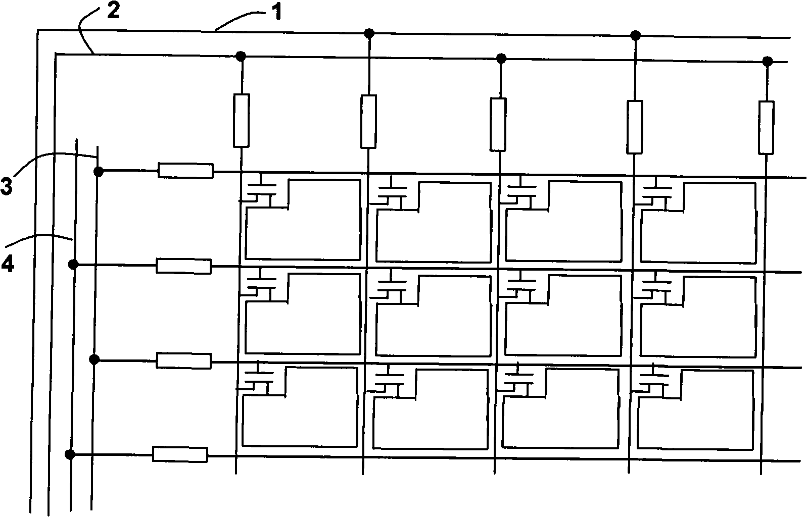
[0071] A glass substrate 37 is provided, provided with a plurality of liquid crystal display panel units and peripheral test circuit areas, a first metal layer 38 is deposited on the glass substrate 37 and a first metal interconnection pattern is etched, the pattern includes The first and second data short-circuit bar wirings 1 and 2 to be connected to the data wiring in the unit extend to the gate wiring in the corresponding peripheral test circuit area,

[0072] An insulating layer 39 and a semiconductor layer 40 are sequentially deposited on the interconnect pattern, and a first photoresist layer 41 is coated,

[0073] The first photoresist layer 41 is subjected to multi-grayscale exposure, so that in the test circuit area, the gate wiring will overlap with the gate shorting bars 3, 4 and the area where the data shorting bars will be electrically connected ...

Embodiment 2

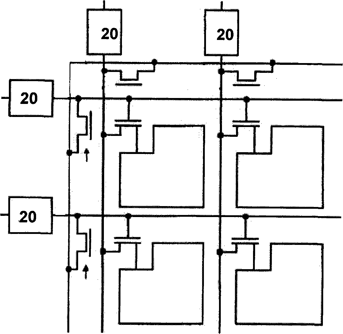
[0083] A manufacturing method of a liquid crystal display device and a TFT completed substrate, the method and structure of which are basically the same as those of Embodiment 1, and electrostatic protection rings 20 are also provided at the terminals of gate wiring and data wiring. Through the conduction effect of the Guard transistors in these electrostatic protection rings 20, the electrostatic protection in the panel after the completion of the entire array process is realized. After the array process is completed and the panel is cut, the electrostatic protection ring 20 in the panel can still be used to protect against static electricity. In order to protect the purpose of static electricity in all process steps.

Embodiment 3

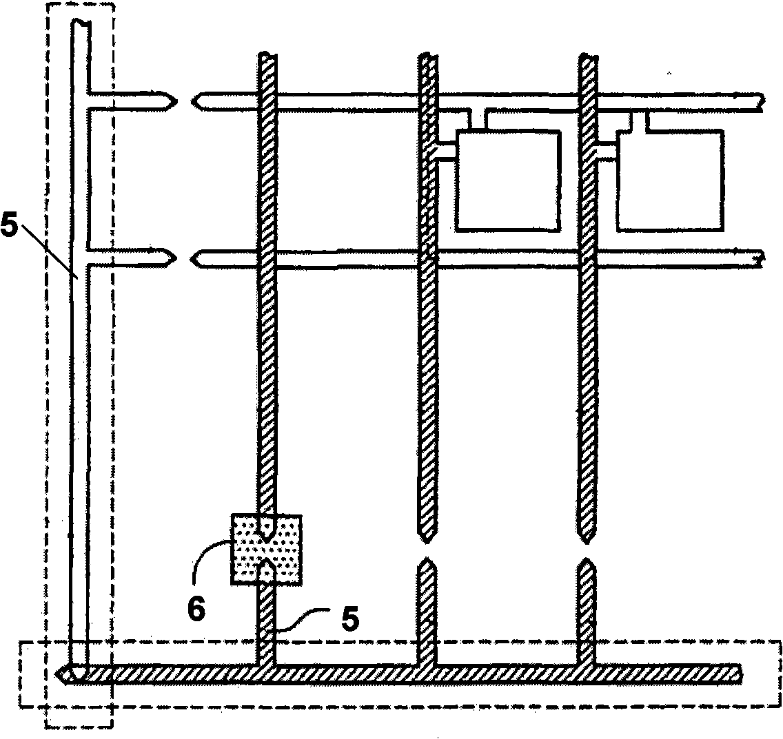
[0085] A manufacturing method of a liquid crystal display device and a TFT completed substrate, the method and structure of which are basically the same as in Embodiment 1, the shorting bar traces 1, 2, 3, and 4 are respectively connected to the array test pads 31 of each panel, and The test terminals of the array test pad groups of different panels on all TFT substrates are connected to each other in order through the auxiliary protective wiring 30 , and connected to the total array test pad group 32 .

[0086] In this way, at the moment when static electricity is generated, the local electrostatic charge can be diffused to the whole large glass substrate to the greatest extent; at the same time, due to the array test structure interconnected between panels, the array test of different products can use the same A set of probes saves the cost of probe development and shortens the product development time to a large extent.


PUM


Abstract

The present invention relates to a Mfg. method for liquid-crystal display and a TFT complete substrate, the manufacturing method etch the insulation layer and the semi-conductor layer between two-layer metallic layers by using multi- gray level light shield at the overlap joint of the spacing layer circuit in the electrostatic protecting loop to folding electrically connect the two-layer metallic layer directly. The structure and the manufacturing method can interconnect with the first floor metal directly to share the same electric potential when the second metallic layer film is formed, the unused electrostatic charge is shared by both, and the discharging phenomenon between two-layer metal is prevented. The formed time of the effective electrostatic protection is ahead of time.

Description

technical field [0001] The invention relates to a semiconductor element and a manufacturing method, in particular to a manufacturing method of a thin film transistor liquid crystal display device and a TFT completed substrate, on which a plurality of liquid crystal display panel units are arranged. Background technique [0002] A liquid crystal display (liquid crystal display, LCD) is currently the most widely used type of flat panel display, and has the characteristics of low power consumption, thin appearance, light weight, and low driving voltage. The liquid crystal display module is mainly composed of a liquid crystal display panel and a backlight module. Wherein, the liquid crystal display panel is generally composed of a thin film transistor array substrate (TFT substrate), a color filter film substrate (CF substrate), and a liquid crystal layer disposed between them. The backlight module is used to provide the surface light source required by the liquid crystal displ...

Claims


Application Information

Patent Timeline
Patent Type & Authority Applications(China)
IPC IPC(8): H01L21/84H01L21/768H01L27/12H01L23/522H01L23/60G02F1/1362G02F1/133G03F7/00
Inventor 徐华伟
Owner NANJING CEC PANDA LCD TECH
Why Eureka
Try Eureka