Electrostatic protection component, and electronic component module using the same
A technology for electronic components and resistance parts, applied in electrical components, electric solid state devices, circuits, etc., can solve the problems of no heat dissipation mechanism, difficult heat dissipation of light-emitting diodes, etc., and achieve thinning, excellent electrostatic pulse resistance, and heat dissipation. excellent effect
- Summary
- Abstract
- Description
- Claims
- Application Information
AI Technical Summary
Problems solved by technology
Method used
Image

Examples
Embodiment approach 1
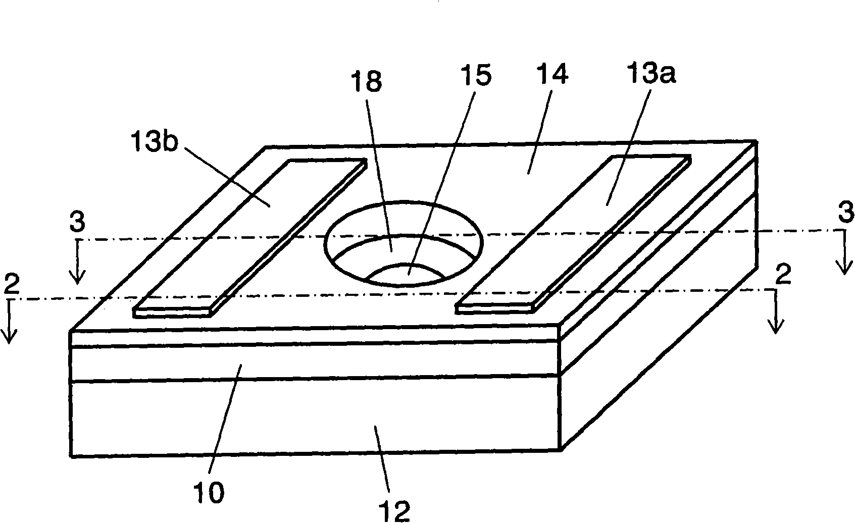
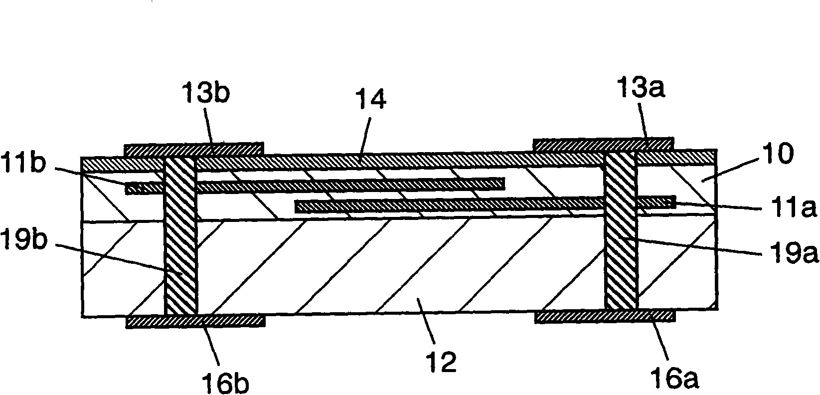
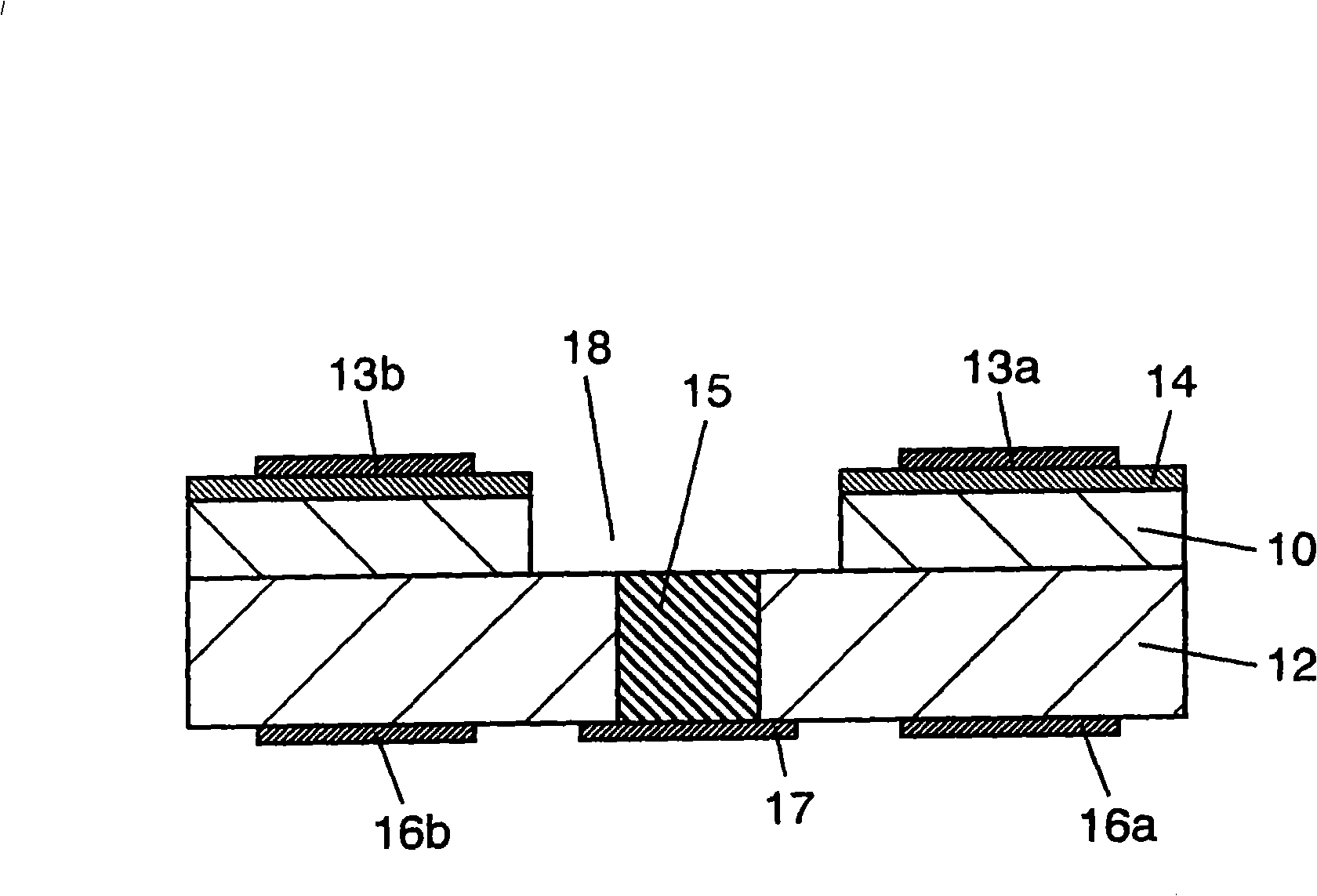
[0036] figure 1 It is an external perspective view of the static electricity countermeasure component according to Embodiment 1 of the present invention. figure 2 It is a cross-sectional view taken along line 2-2 of the static electricity countermeasure component of this embodiment. image 3 It is a cross-sectional view taken along line 3-3 of the static electricity countermeasure component of this embodiment. Figure 4 It is a schematic exploded perspective view of the static electricity countermeasure part of this embodiment. Figure 5 It is a sectional view of the light emitting diode module of this embodiment. Image 6 It is an equivalent circuit diagram of the light emitting diode module of this embodiment.
[0037] Such as figure 1 , figure 2 , image 3 with Figure 4 As shown, the static electricity countermeasure component of the present embodiment has a variable resistance unit 10 in which three variable resistance layers 10a, 10b, and 10c and internal electr...
Embodiment approach 2
[0068] The difference between Embodiment 2 and Embodiment 1 is that, in Embodiment 1, the external electrodes 16a and 16b are formed on the surface of the ceramic substrate 12 on which the terminal electrodes 13a and 13b are not formed. External electrodes 16a and 16b are formed on the side surfaces of the varistor unit 10 and the ceramic substrate 12 .
[0069]Hereinafter, the static electricity countermeasure member and light emitting diode module according to Embodiment 2 of the present invention will be described.
[0070] Figure 12 It is an external perspective view of the static electricity countermeasure component of this embodiment. Figure 13 It is the electrostatic countermeasure part of this embodiment Figure 12 Sectional view of A-A'. Figure 14 It is the electrostatic countermeasure part of this embodiment Figure 12 Sectional view of B-B'. Figure 15 It is a schematic exploded perspective view of the static electricity countermeasure part of this embodimen...
PUM
| Property | Measurement | Unit |
|---|---|---|
| Thickness | aaaaa | aaaaa |
| Thickness | aaaaa | aaaaa |
| Thickness | aaaaa | aaaaa |
Abstract
Description
Claims
Application Information
 - Generate Ideas
- Intellectual Property
- Life Sciences
- Materials
- Tech Scout
- Unparalleled Data Quality
- Higher Quality Content
- 60% Fewer Hallucinations
Browse by: Latest US Patents, China's latest patents, Technical Efficacy Thesaurus, Application Domain, Technology Topic, Popular Technical Reports.
© 2025 PatSnap. All rights reserved.Legal|Privacy policy|Modern Slavery Act Transparency Statement|Sitemap|About US| Contact US: help@patsnap.com