Method for improving MOSFET anti-single particle radiation and MOSFET component

A technology for anti-single particle radiation and devices, which is applied in the manufacture of semiconductor devices, electric solid devices, semiconductor/solid devices, etc., can solve problems such as increased leakage current, not an anti-irradiation method, and weakened STI isolation ability, etc., to achieve Realize the effect of simple process and suppression of micro-dose effect

Inactive Publication Date: 2008-09-17
PEKING UNIV
View PDF0 Cites 2 Cited by
  • Summary
  • Abstract
  • Description
  • Claims
  • Application Information

AI Technical Summary

Problems solved by technology

But this method is not a feasible anti-irradiation method, because it will seriously weaken the isolation ability of STI, which will increase the leakage current between devices in integrated circuits

Method used


Image

  • Method for improving MOSFET anti-single particle radiation and MOSFET component
  • Method for improving MOSFET anti-single particle radiation and MOSFET component
  • Method for improving MOSFET anti-single particle radiation and MOSFET component

Examples


Embodiment Construction

[0026] Below in conjunction with accompanying drawing and specific embodiment the present invention is described in further detail:

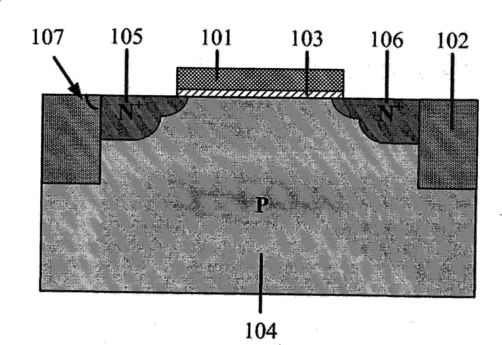
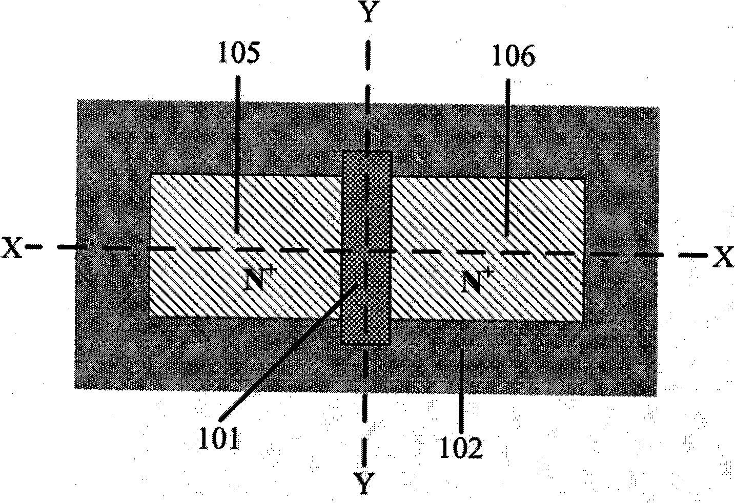
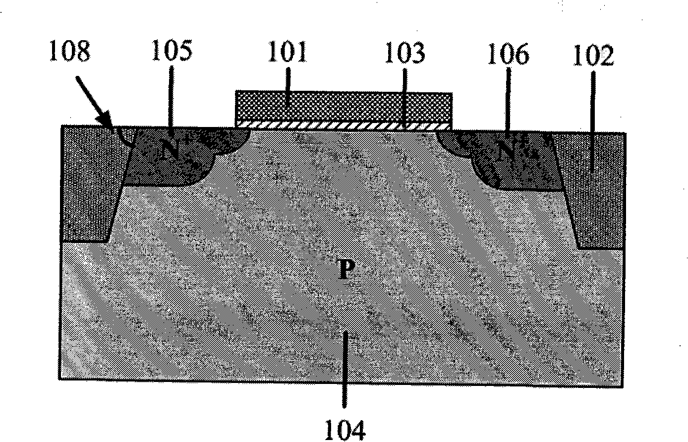
[0027] figure 2 , image 3 with Figure 4 It is a structural schematic diagram of a specific embodiment of the transistor of the present invention, and the structure of the device includes: 101-gate, 102-isolation region of the device, 103-gate oxide layer, 104-P-type silicon substrate, 105-source (drain) ), 106-drain (source), 108-the angle between the sidewall of the trench in the STI region and the upper surface of the active region of the device in the optimized MOSFET structure. The channel length of the device is 130 nanometers, the thickness of the gate oxide is 3 nanometers, the depth of the isolation structure is 400 nm, and the inclination angle of the trench side wall is 85 degrees.

[0028] The following combination Figure 5 to Figure 8 And take NMOSFET as an example to briefly describe an implementation method for preparing th...


PUM


Abstract

The invention discloses a method for enhancing anti-single particle radiation ability of MOSFET and a MOSFET element, belonging to field effect transistor technology field. In the MOSFET element according to the invention, an acute angle between the side wall of channel in STI region and the active region of the element is defined as the angle of micro-dosage effect caused by the anti-single particle radiation of the element, with value ranged between 78 degrees to 86 degrees. By using the MOSFET element structure according to the invention, the off-state leakage current of the element caused by the single-particle radiation is lower than that the traditional structure by one magnitude. The structure according to the invention has simple process, completely compatible with traditional CMOS process, capable of enhancing the anti-single particle radiation ability of the element and effectively reducing the manufacturing costs simultaneously.

Description

technical field [0001] The invention relates to a MOSFET device in the field of field effect transistor (MOSFET-Metal Oxide Silicon Field Effect Transistor, MOSFET for short), in particular to a method for improving the MOSFET's anti-single particle irradiation and a MOSFET device. Background technique [0002] In the standard MOSFET process, as the feature size of the device decreases, the shallow trench isolation structure (STI) gradually replaces the local oxidation isolation structure (LOCOS) and becomes the mainstream isolation structure. According to the requirements of the International Semiconductor Technology Roadmap (ITRS), the sharp angle between the sidewall of the STI trench and the upper surface of the active region of the device should be as steep as possible. Therefore, according to the ITRS updated in 2006, for the MOSFET process in 2008, the value of the acute angle between the sidewall of the STI trench and the upper surface of the active region of the dev...

Claims


Application Information

Patent Timeline
Patent Type & Authority Applications(China)
IPC IPC(8): H01L27/02H01L29/78H01L21/762
Inventor 王鹏飞黄如鲁庆
Owner PEKING UNIV
Why Eureka
Try Eureka