Organic film transistor and its making method

A technology of organic thin film and manufacturing method, which is applied in semiconductor/solid-state device manufacturing, electrical solid-state devices, semiconductor devices, etc., can solve the problems of limiting the development of organic transistors, short life, poor electrical properties of devices, etc., to improve stability, The effect of improving transfer ability and reducing hydroxide density

Inactive Publication Date: 2008-09-17
AU OPTRONICS CORP
View PDF0 Cites 11 Cited by
  • Summary
  • Abstract
  • Description
  • Claims
  • Application Information

AI Technical Summary

Problems solved by technology

[0006] However, in organic thin film transistors, most of the organic semiconductor materials are P materials. At present, P-type organic transistors have higher carrier mobility and less N-type materials. It is necessary to find N-type materials with comparable carrier mobility and Not much, in addition, the current common N-type organic semiconductor materials are easily affected by water vapor or oxygen when operating in the air, resulting in poor electrical properties of the device and a relatively short life
Therefore, most of the current N-type organic thin film transistors must be operated in nitrogen or vacuum, which limits the further development of organic transistors.

Method used


Image

  • Organic film transistor and its making method
  • Organic film transistor and its making method
  • Organic film transistor and its making method

Examples


Embodiment Construction

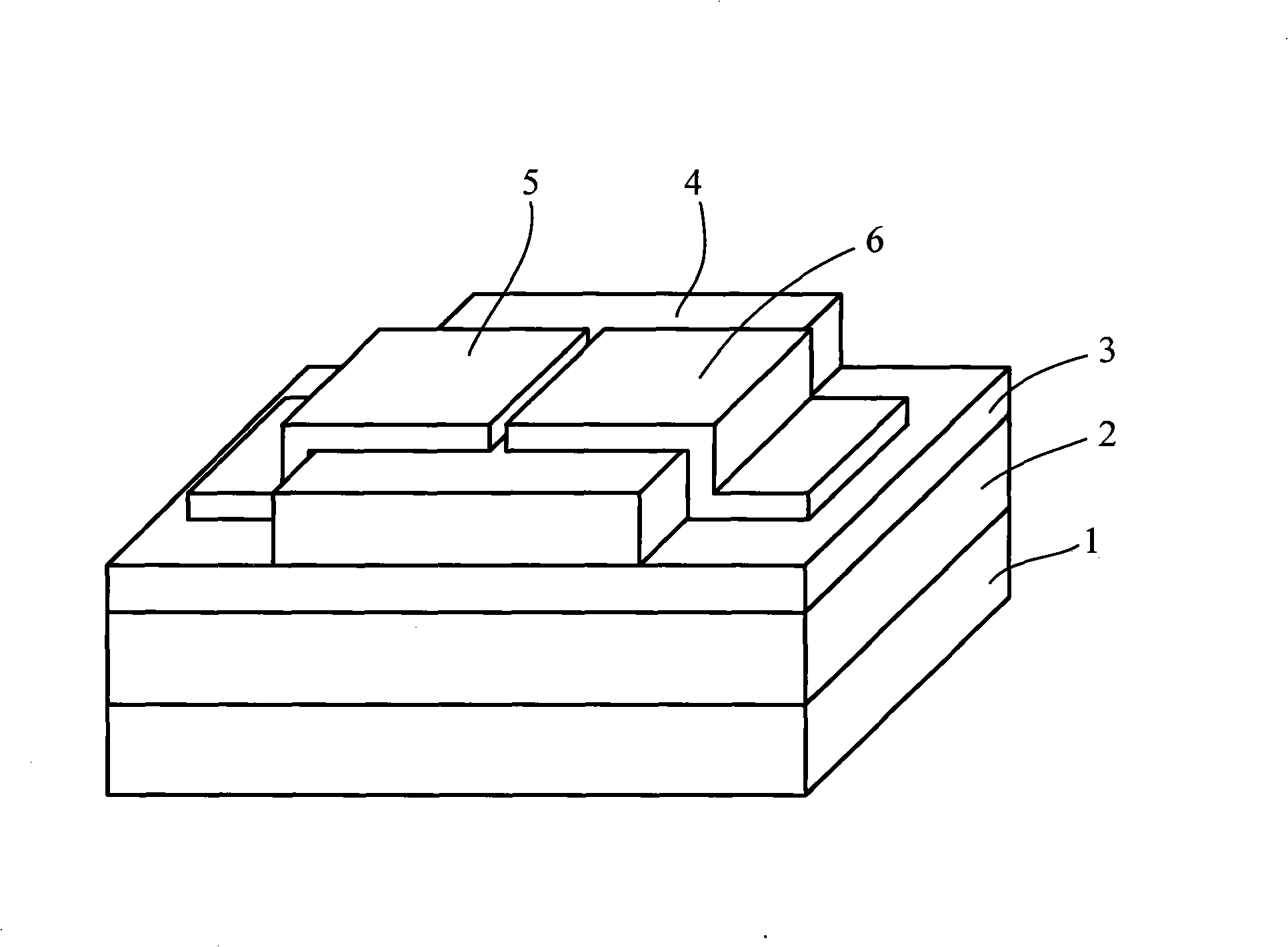
[0020] Please refer to figure 1 , is a schematic diagram of the unpackaged structure of the organic thin film transistors (OTFT) of the present invention. The OTFT of the present invention includes a gate 1, a gate insulating layer 2, an organic modified insulating layer (polymer insulator) 3, and source layer 4 , source electrode 5 and drain electrode 6 . In this embodiment, the OTFT of the present invention is an N-type OTFT, and the active layer 4 is an N-type organic semiconductor layer (eg, formed of PTCDI-C8 material). Before the N-type organic semiconductor layer 4 is formed in the OTFT of the present invention, an organic modified insulating layer 3 is formed by spin coating on the surface of the gate insulating layer 2, and then N is deposited on the organic modified insulating layer 3 by thermal evaporation. The N-type organic semiconductor layer 4 is formed by forming a film of an N-type material. Through the surface modification of the organic modified insulating...


PUM


Abstract

The invention relates to an organic thin-film transistor and the making method, wherein the organic thin-film transistor comprises a gate electrode, a gate insulation layer, an active layer, a source electrode and a drain electrode, the organic thin-film transistor also comprises an organic modification insulation layer which is located on the surface of the gate insulation layer. The organic thin-film transistor of the invention uses the organic modification insulation layer to modify the gate insulation layer properly, and the organic thin-film transistor can provide good contact surface for N-type thin-film transistor, and reduce the interface by which electron are limited in the active layer and the gate insulation layer, and reduce hydroxyl density, then enhance transmission capacity of the electron in channel, and can improve stability of the organic thin-film transistor in atmospheric environment.

Description

【Technical field】 [0001] The invention relates to a thin film transistor and its manufacturing method, especially to an N-type organic thin film transistor and its manufacturing method. 【Background technique】 [0002] The traditional inorganic transistor is a metal oxide semiconductor (MOS) type field effect transistor, and its semiconductor material is generally inorganic silicon. Organic thin film transistors (OTFT) are also called plastic transistors. The biggest difference from MOS transistors is that OTFT uses organic semiconductor materials instead of inorganic semiconductor materials in MOS. [0003] Compared with inorganic transistors, organic thin film transistors have the following main advantages: there are more and newer film-forming technologies for organic thin films, such as Langmuir-Blodgett (LB) technology, molecular self-assembly technology, vacuum evaporation, inkjet printing, etc., thus The manufacturing process is simple, diverse, and low-cost; the size...

Claims


Application Information

Patent Timeline
Patent Type & Authority Applications(China)
IPC IPC(8): H01L51/05H01L51/40
Inventor 陈方中廖呈祥黄昱仁黄维邦黄伟明
Owner AU OPTRONICS CORP
Why Eureka
Try Eureka