

Flip-chip light emitting diodes and method of manufacturing thereof
A flip-chip, light-emitting device technology, applied in electrical components, circuits, semiconductor devices, etc., can solve problems such as low luminous efficiency and low adhesion, and achieve increased packaging yield, low contact resistivity, and excellent current-voltage. Effects of Features
- Summary
- Abstract
- Description
- Claims
- Application Information
AI Technical Summary
Problems solved by technology
Method used
Image

Examples
Embodiment Construction
[0052] Hereinafter, a flip-chip nitride-based light emitting device according to a preferred embodiment of the present invention will be described in more detail with reference to the accompanying drawings.
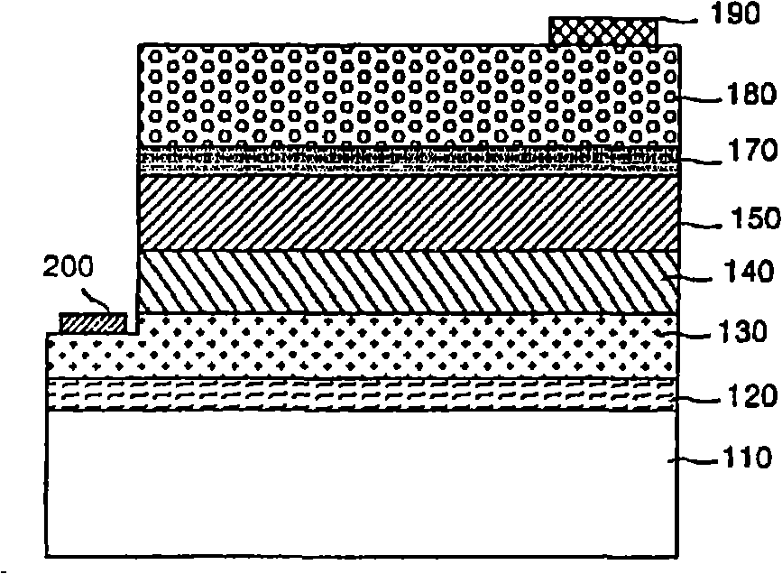
[0053] figure 1 A cross-sectional view of a flip-chip nitride-based light emitting device according to a first embodiment of the present invention is shown.
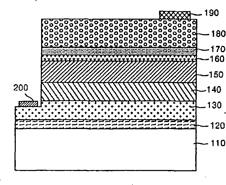
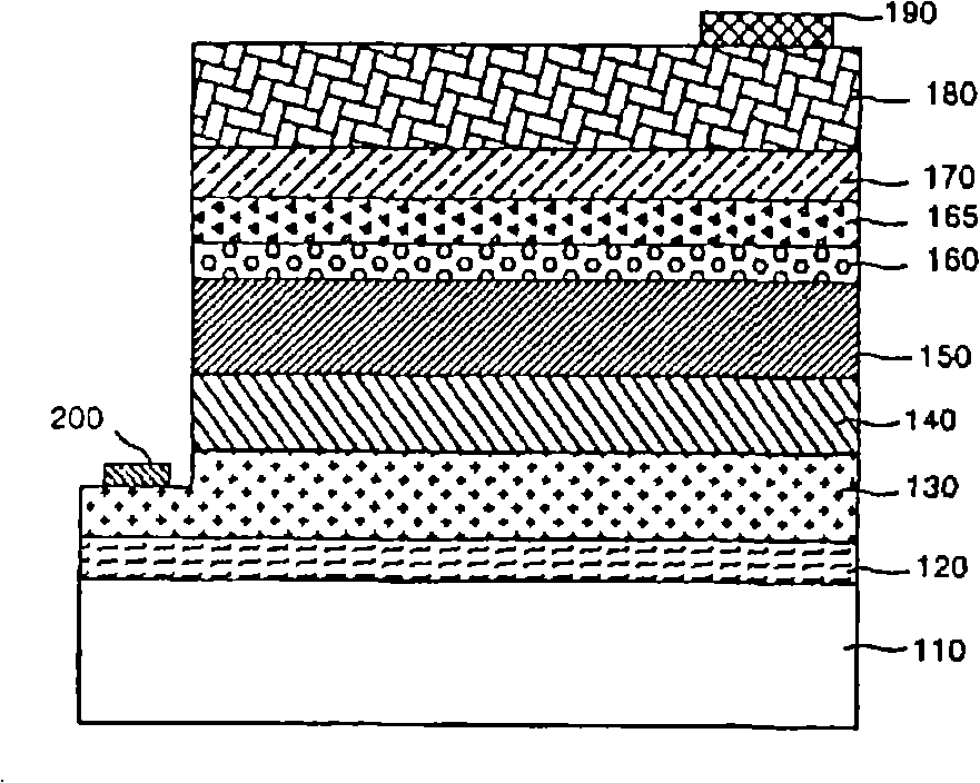
[0054] now refer to figure 1 , a flip-chip nitride-based light-emitting device is formed by the following structure, which includes a substrate 110, a buffer layer 120, an n-type cladding layer 130, an active layer 140, a p-type cladding layer sequentially stacked thereon. layer 150, transparent conductive film layer 170 and reflective layer 180. Reference numerals 190 and 200 denote p-type electrode pads and n-type electrode pads, respectively.
[0055] The part from the substrate 110 to the p-type cladding layer 150 corresponds to a light-emitting structure, and the transparent conductive film layer 170 stacked...
PUM
| Property | Measurement | Unit |
|---|---|---|
| Thickness | aaaaa | aaaaa |
| Thickness | aaaaa | aaaaa |
Abstract
Description
Claims
Application Information