
Phase-change memorizer 1R1T structure and its driver circuit design method

A phase change memory, 1R1T technology, applied in static memory, read-only memory, digital memory information and other directions, can solve the problems of high cost, unfavorable integration of phase change memory, large area, etc., to increase the implementation method, increase the scale and complexity performance, and the effect of reducing manufacturing costs

Inactive Publication Date: 2008-10-15
SHANGHAI INST OF MICROSYSTEM & INFORMATION TECH CHINESE ACAD OF SCI
View PDF0 Cites 6 Cited by
  • Summary
  • Abstract
  • Description
  • Claims
  • Application Information

AI Technical Summary

Problems solved by technology

But this puts higher requirements on the process line, because both ends of the GST material need to have MOS tubes, and the phase change material GST must be integrated into the process line during manufacturing, which puts higher requirements on the process line. The cost is huge; or do not integrate GST into the CMOS process line, that is, first use the standard CMOS (Complementary Metal Oxide Semiconductor) process to make the circuit part, and finally use the GST process line to make the GST material, because the gate tube is the source Grounded, so a very long metal lead is required to connect the GST on the top layer to the gate transistor on the bottom layer, and the last layer of connecting metal still needs a large area, which is not conducive to the integration of phase change memory

Method used


Image

  • Phase-change memorizer 1R1T structure and its driver circuit design method
  • Phase-change memorizer 1R1T structure and its driver circuit design method
  • Phase-change memorizer 1R1T structure and its driver circuit design method

Examples


Embodiment Construction

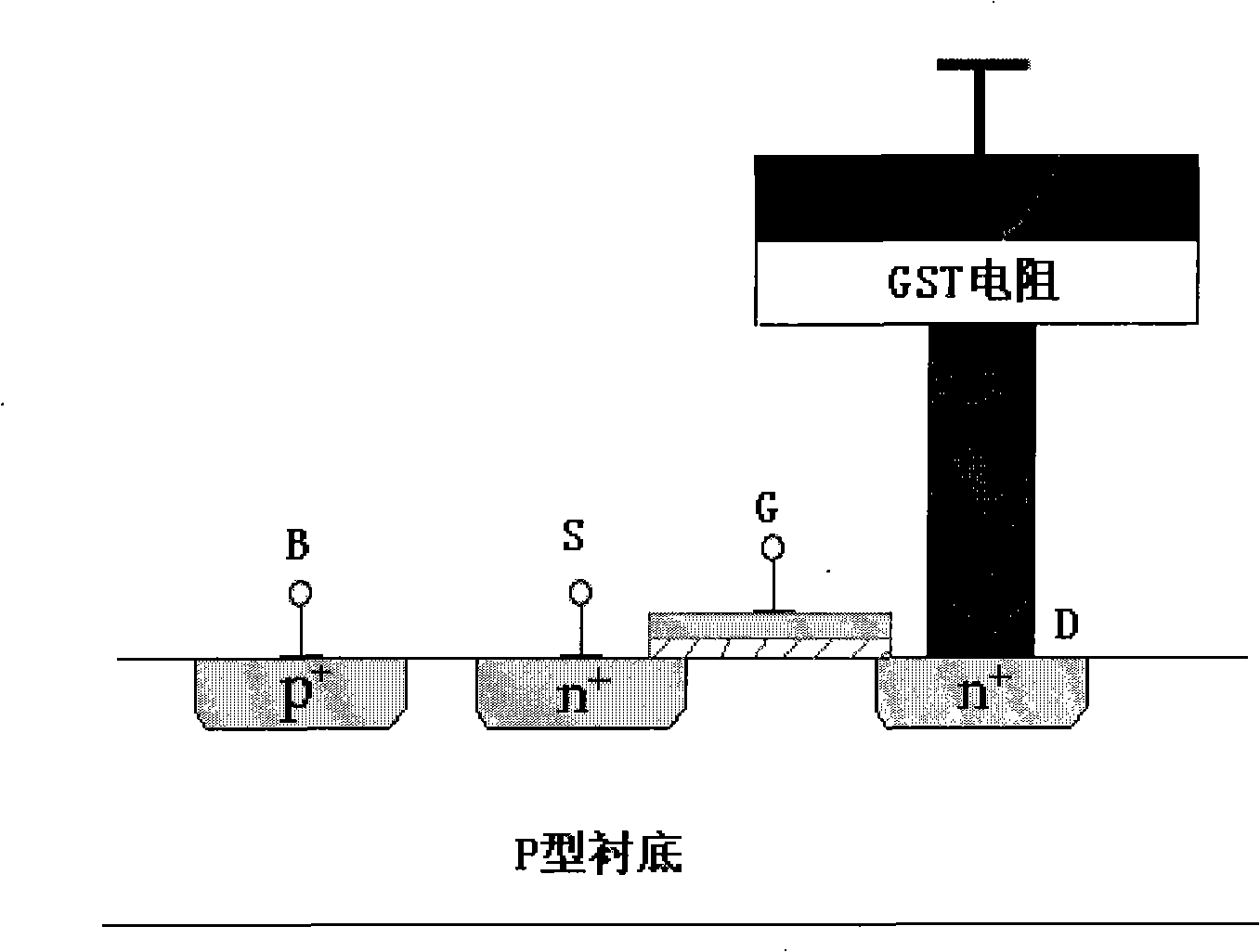
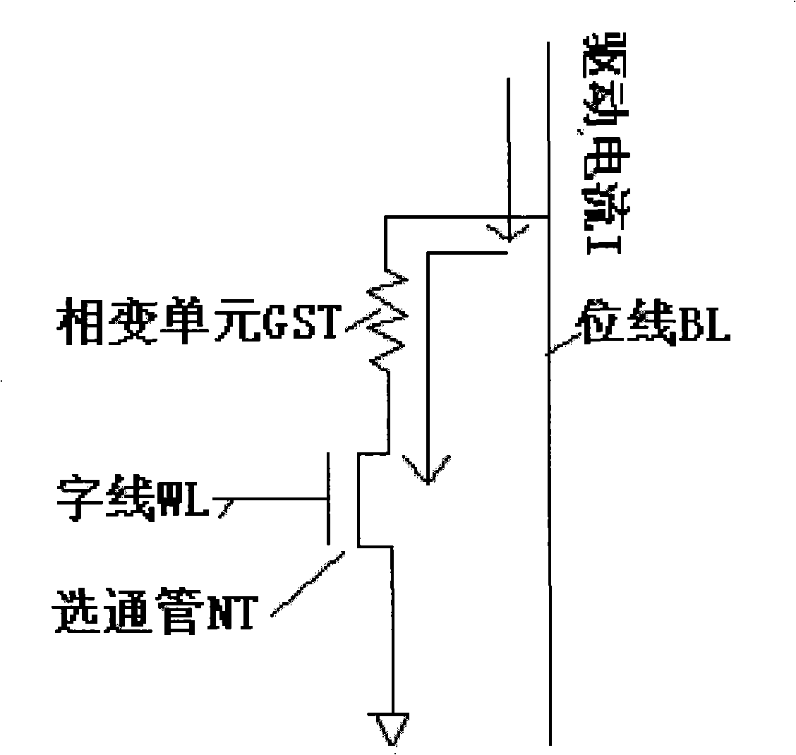
[0032] A specific embodiment of the specific implementation of 1R1T of the present invention, such as Figure 4 As shown, first the basic circuit part is completed through the standard CMOS process line, the drain end of the gate tube is connected through the outermost layer of metal, and then SiO is deposited on the layer of metal 2And etch a smaller through hole 3, and fill it with metal tungsten (as the lower electrode), and next to this smaller through hole is another slightly larger through hole 4, so far, all are completed by standard CMOS technology of. Then use the GST process line, first sputter a layer of phase change material GST to cover the larger through hole above, and then etch away the excess GST, (a layer of SiO can be added 2 ), and then grow a layer of metal aluminum (Al) on it as the upper electrode 5, etch, and finally cover a passivation layer of silicon dioxide.

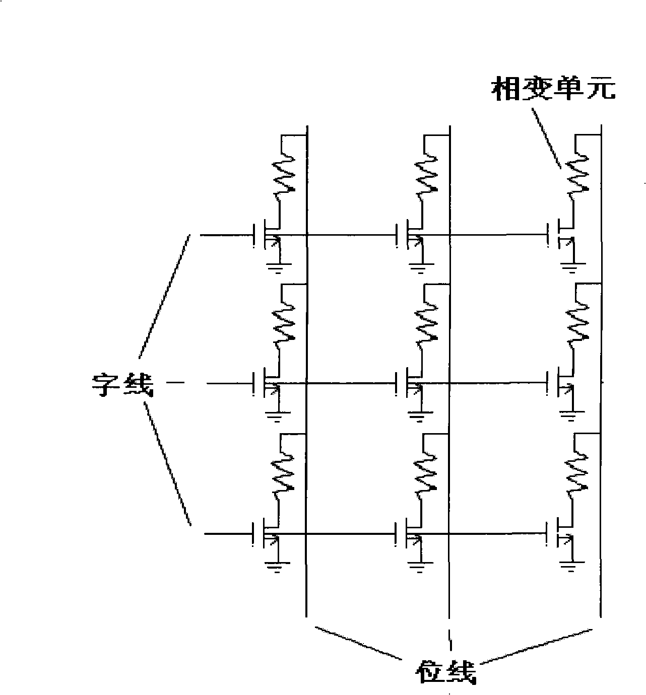
[0033] In this way, except for the phase change resistor GST part in the storage array, ...


PUM


Abstract

The invention relates to a design method of a phase-change storage 1R1T structure and a drive circuit that is used by the phase-change storage 1R1T structure. The invention is characterized in that an IRIT structure that interconnects a phase-change resistance GST and an NMOS gate tube in a certain way is adopted, and based on the adopted IRIT structure, the design method of the drive circuit is disclosed and is characterized in that the source end of the gate tube is connected with one end of the drive circuit, the leakage end of the gate tube is connected with the phase-change resistance, the grid end of the gate tube is connected with the bit line of a phase-change array, the other end of the phase-change resistance is connected with the highest power level VDD of the circuit. A double-level current mirror circuit is adopted, wherein, the first level comprises three current mirrors that are formed by three pairs of PMOS tubes, the second level comprises three current mirrors that are formed by three pairs of NMOS tubes, and the double-level current mirror circuit is finally coupled with the bit line, thus generating a drive current that is used for reading, writing and erasing, and applied to the phase-change storage unit. Under the precondition that the complexity and the scale of circuit design are not increased, the design method of the drive circuit obtains the effects of lowering the requirements of the technical production line and production cost.

Description

technical field [0001] The invention belongs to the technical field of large-scale integrated circuits, and specifically relates to a new 1R1T structure design and its corresponding drive circuit design mainly composed of a two-stage current mirror structure. Background technique [0002] Chalcogenide-Random Access Memory (C-RAM, Chalcogenide-Random Access Memory) technology is based on the Ovshinsky electronic effect proposed by S.R.Ovshinsky in the 1960s and 1970s. Ovonics Unified Memory (OUM-Ovonics Unified Memory). The basic principle of phase-change memory is: reversible phase-change materials processed to nanometer size, using the low resistance in the crystalline state of the material and the high resistance in the amorphous state to realize storage in different states. The phase change unit in the phase change memory uses very little material, has high storage density and is easy to manufacture. It can be manufactured by adding only 2-4 mask steps to the existing st...

Claims


Application Information

Patent Timeline
IPC IPC(8): G11C11/56G11C16/02G11C16/06G05F3/26
Inventor 宋志棠沈菊刘波封松林
Owner SHANGHAI INST OF MICROSYSTEM & INFORMATION TECH CHINESE ACAD OF SCI
Features
  • Generate Ideas
  • Intellectual Property
  • Life Sciences
  • Materials
  • Tech Scout
  • Unparalleled Data Quality
  • Higher Quality Content
  • 60% Fewer Hallucinations
Learn More