

Semiconductor integrated circuit and layout method for the same
A technology of integrated circuits and semiconductors, which is applied in the fields of semiconductor devices, semiconductor/solid-state device manufacturing, and semiconductor/solid-state device components, etc. It can solve the problems of large chip clock skew, large wiring resistance, and inability to calculate high-precision delays. Achieve the effect of small clock offset and low power consumption
Inactive Publication Date: 2008-10-22
PANASONIC CORP
View PDF3 Cites 14 Cited by
- Summary
- Abstract
- Description
- Claims
- Application Information
AI Technical Summary
Problems solved by technology
However, the comb-type clock wiring can control the deviation of the wiring delay so that the circuit does not malfunction to prevent a decrease in operating speed, but if the flip-flops on the output side and the receiving side of the signal are one-to-one, it can be controlled The deviation of wiring delay, but in general circuits, due to the many-to-many relationship, it is very difficult to control the deviation of all flip-flops to wiring delay
In addition, although the herringbone clock is effective when the chip size is small, in a large-scale semiconductor integrated circuit, the branch wiring in the horizontal direction is long, and the wiring resistance from the center to the end of the branch wiring is extremely high. Large, there is a problem that the clock skew between the center of the chip and the periphery of the chip increases due to the deviation of the wiring delay
In addition, since many clock synchronization units are connected to the clock backbone wiring as loads, there is also a problem that the variation in the wiring delay of the clock backbone wiring is also large.
In addition, in the mesh type clock, since the clock is wired in a grid pattern for the entire block, the wiring resistance is small, and the variation of wiring delay is small, but there is a problem that the total wiring length of the clock is long, and the load on the clock driving unit that supplies the clock signal Large capacity, large power consumption
In this case, if there is a clock skew before multiple clock driving units, the through current will flow between the clock driving units through the herringbone clock wiring and mesh wiring, and there is a problem that the power consumption will increase.
In addition, in the delay calculation tool currently available on the market at the standard cell level, when one clock line is driven by multiple clock drive units like this, there is a problem that the delay calculation cannot be performed with high precision. Cannot account for the effects of crosstalk with other signal routing
In addition, in order to reduce the wiring delay of the clock signal, if the upper layer wiring with a thick film thickness and low resistance is used, it is necessary to use a wide wiring due to the limitation of the manufacturing process. Contact) is large, and if it is used for the entire clock wiring, the signal wiring area is insufficient, so it becomes difficult to use the upper layer wiring at the end side of the clock tree that drives many clock driving units or clock synchronization units
Method used
View moreImage
Smart ImageViewing Examples

Examples
no. 1 approach
no. 2 approach
no. 3 approach
Login to View More PUM
 Abstract
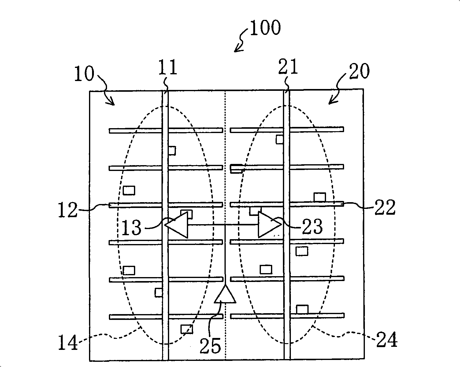
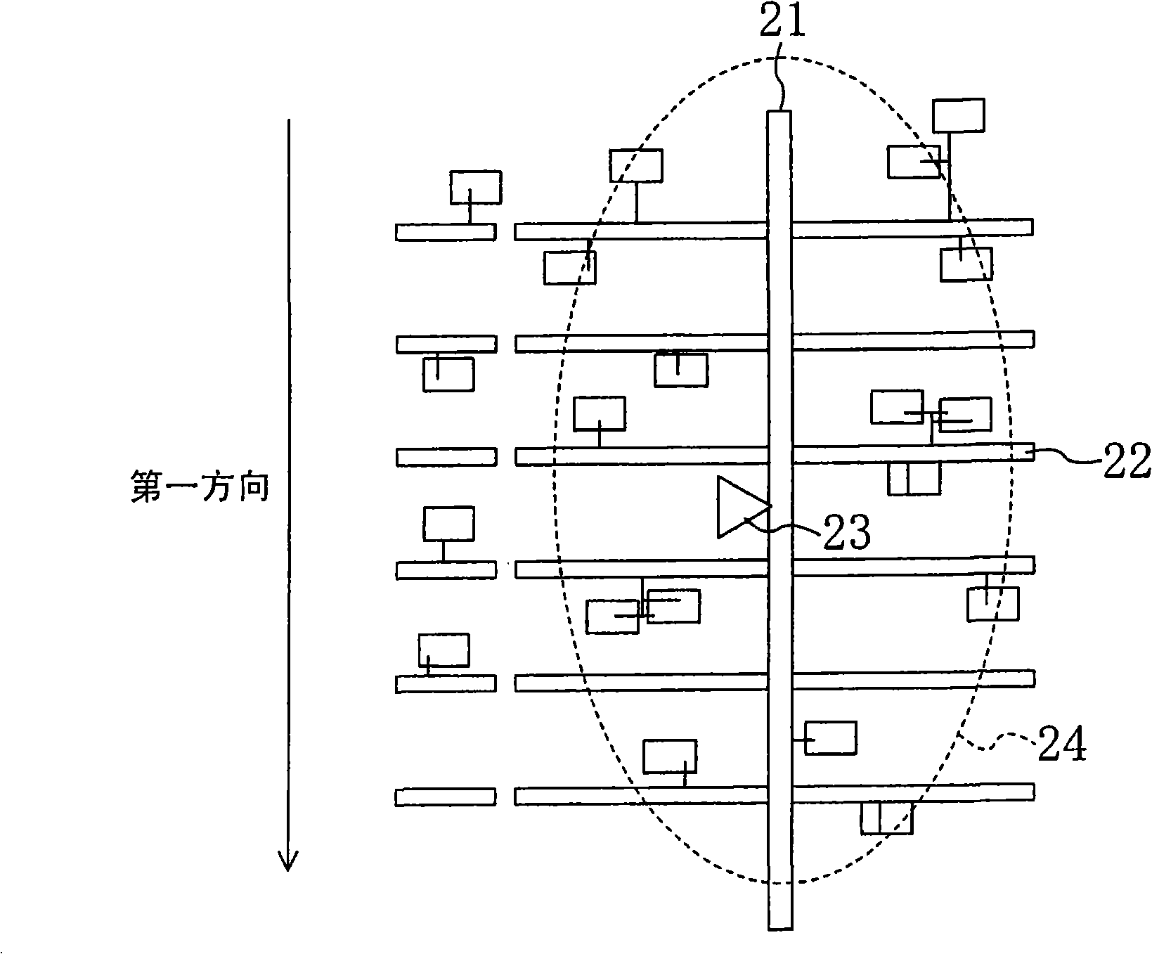
A functional block is divided into a plurality of regions. In each region, a clock main line extending along a first direction, a clock branch line group including a plurality of clock branch lines extending along a second direction perpendicular to the first direction and electrically connected to the clock main line, a clock driving cell electrically connected to the clock main line and a clock synchronous cell group including a plurality of clock synchronous cells electrically connected to the clock main line or the clock branch line group are provided. The clock branch line groups of the respective regions are electrically separated from each other, and the clock driving cell singly drives the clock main line connected thereto and the clock branch line group connected to the clock main line.
Description
Semiconductor integrated circuit and layout method of semiconductor integrated circuit technical field The present invention relates to a semiconductor integrated circuit using a clock distribution circuit for distributing clock signals in functional blocks constituted by standard cells, and a layout method of the semiconductor integrated circuit. Background technique In recent years, along with the increase in speed and function of digital circuits, the increase in speed and integration of semiconductor integrated circuits has been progressing. As the speed of semiconductor integrated circuits increases, it becomes important to suppress variation in signal delay (clock skew) of a clock signal that synchronizes flip-flops in the semiconductor integrated circuit. Clock skew refers to the difference in the arrival time of clock signals between synchronized flip-flops. If the clock skew is large, there is a problem that the operating frequency will decrease, which in turn wi...
Claims
Login to View More Application Information
Patent Timeline
 Patent Type & AuthorityApplications(China)
IPC IPC(8): G06F17/50H01L27/02H01L23/528H01L21/82H01L21/768
Inventor堤正范吉永生
OwnerPANASONIC CORP