Semiconductor encapsulation construction

A semiconductor and structure technology, applied in the field of semiconductor packaging structure, can solve the problems of substrate redesign, inconvenience, spilled glue contaminating external pads, etc., and achieves the effect of avoiding glue spillage

Inactive Publication Date: 2008-10-29
POWERTECH TECHNOLOGY
View PDF0 Cites 7 Cited by
  • Summary
  • Abstract
  • Description
  • Claims
  • Application Information

AI Technical Summary

Problems solved by technology

However, the encapsulant will spread on the lower surface of the substrate through the through hole through the substrate, and there is a possibility of overflowing glue contaminating the external pads
In addition, the appearance of the final product is changed, and the circuit structure of the substrate must be redesigned
[0005] It can be seen that the above-mentioned existing semiconductor packaging structure obviously still has inconvenience and defects in structure and use, and needs to be further improved urgently.
In order to solve the above-mentioned problems, the relevant manufacturers have tried their best to find a solution, but no suitable design has been developed for a long time. This is obviously a problem that the relevant industry is eager to solve

Method used


Image

  • Semiconductor encapsulation construction
  • Semiconductor encapsulation construction
  • Semiconductor encapsulation construction

Examples


no. 3 Embodiment

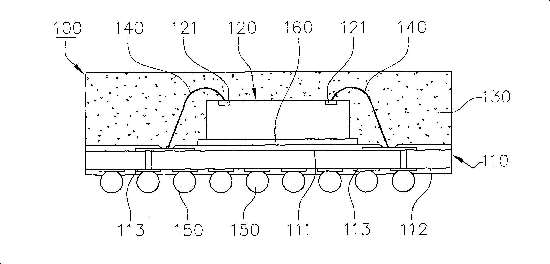
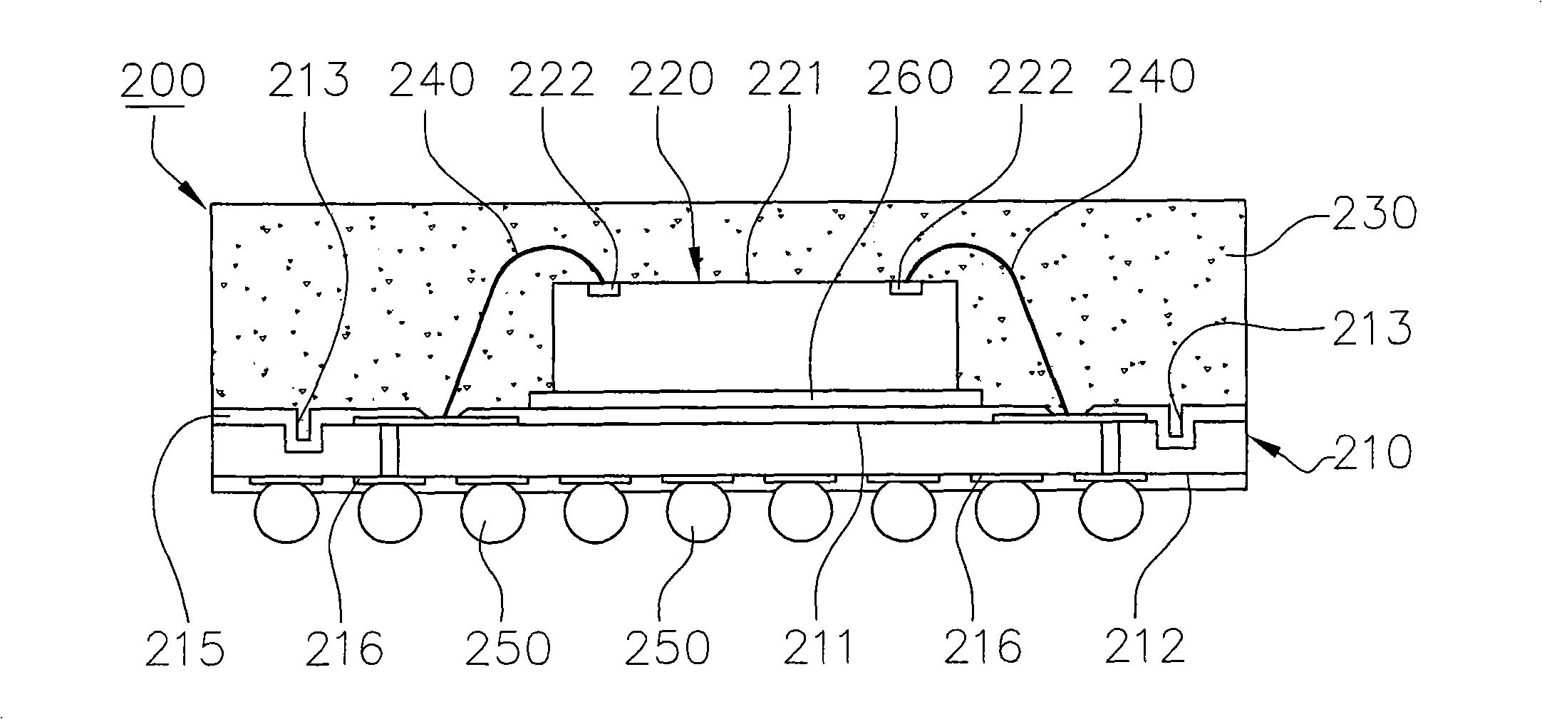
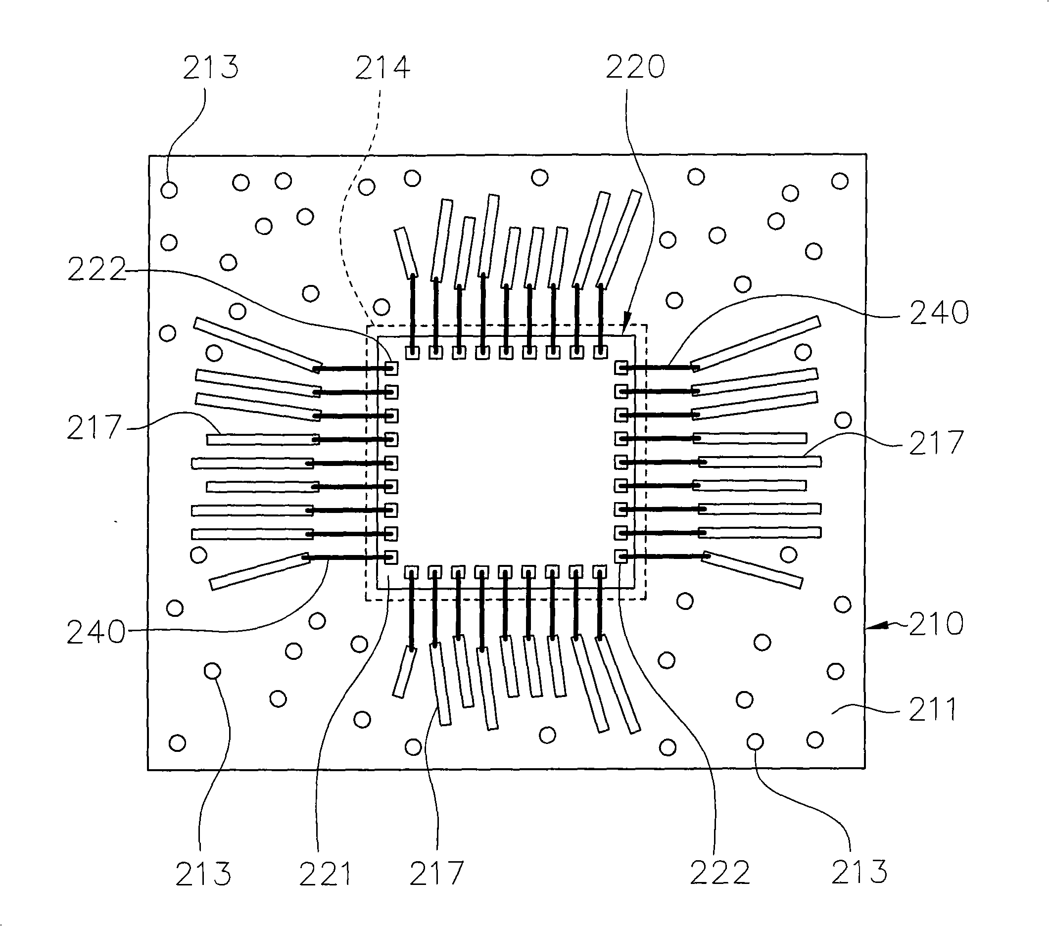
[0080] see Figure 6 Shown is a schematic cross-sectional view of another semiconductor package structure according to the third embodiment of the present invention. Another semiconductor package structure is disclosed in the third embodiment of the present invention. The semiconductor package structure 400 mainly includes a substrate 410 , a chip 420 and an encapsulant 430 .

[0081] The above-mentioned substrate 410 has an upper surface 411 and a plurality of pits 413 formed on the upper surface 411. The upper surface 411 defines a wafer setting area (not shown in the figure), and the pits 413 are located in the The circuit blank area outside the wafer placement area does not penetrate the substrate 410 . The substrate 410 may further include a solder resist layer 414 formed on the upper surface 411 of the substrate 410 and having a plurality of slots 415 to partially expose the upper surface 411 . In this embodiment, the recesses 413 are blind holes that can be located i...


PUM


Abstract

The invention discloses a semiconductor seal structure, comprising a substrate which is provided with an upper surface and a plurality of steel pits formed on the upper surface, the upper surface is defined with a wafer arrangement area, the steel pits are arranged on the blank area of a line outside the wafer arrangement area and do not penetrate the substrate; a wafer which is arranged on the upper surface of the substrate and in the wafer arrangement area; a seal body which is formed on the upper surface of the substrate to seal the wafer; thereby being capable of increasing the seal compound area and the wet air invading paths under the situation of not changing the appearance of a product and reaching the effect that wet air resistance is not peeled off from heat resistance.

Description

technical field [0001] The present invention relates to a semiconductor packaging structure, in particular to a structural design with pits on the substrate, which can increase the bonding area of ​​the sealant and the path of moisture intrusion without changing the appearance of the product, so as to achieve moisture resistance and Heat-resistant, non-peeling, avoiding delamination, and avoiding glue overflow on the ball-mounting surface of the substrate, and there is no need to change the semiconductor package structure (SEMICONDUCTORPACKAGE) of the circuit design of the substrate. Background technique [0002] In existing semiconductor package structures, especially ball grid array packages (Ball Grid Array, BGA), flat pad array packages (Land Grid Array, LGA) or memory card packages (memory card package), the chip is arranged on the substrate and The encapsulant such as epoxy molding compound (EMC) seals it, and the other surface of the substrate is exposed, and a plural...

Claims


Application Information

Patent Timeline
Patent Type & Authority Applications(China)
IPC IPC(8): H01L23/498H01L23/13H01L23/31
CPCH01L2224/16225H01L2224/73204H01L2224/16227H01L2224/4824H01L2224/48227H01L2924/15311H01L2924/1515H01L2224/73265
Inventor 范文正
Owner POWERTECH TECHNOLOGY
Why Eureka
Try Eureka