

MEMS device vacuum encapsulation method
A technology for vacuum packaging and devices, applied in instruments, microstructure devices, processing microstructure devices, etc., can solve the problems of poor electrical interconnection flexibility, difficulty in detecting vacuum degree retention ability, and difficulty in ensuring smooth implementation. cost saving effect
- Summary
- Abstract
- Description
- Claims
- Application Information
AI Technical Summary
Problems solved by technology
Method used
Image

Examples
Embodiment 1
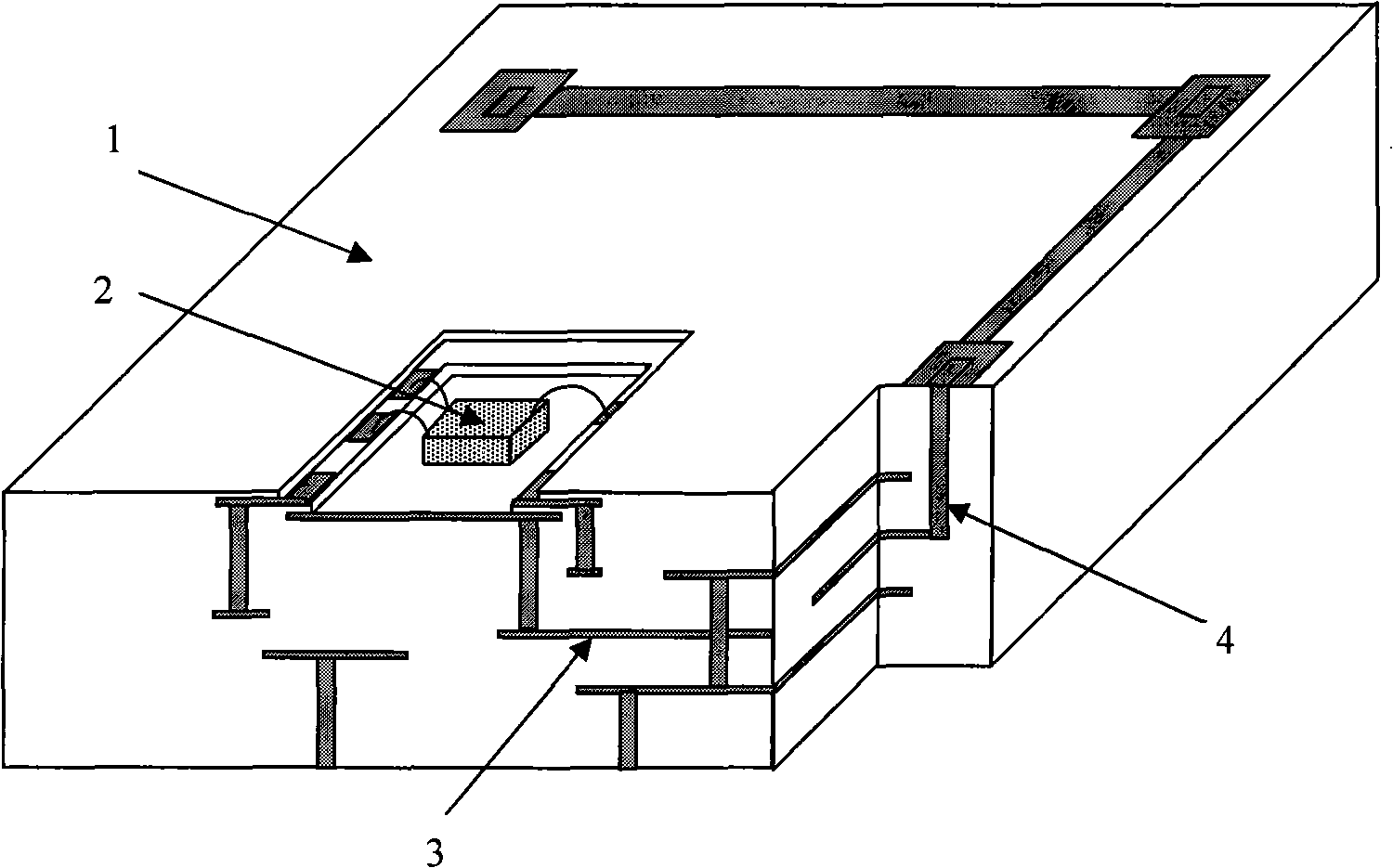
[0043] Using low-temperature co-fired ceramics as the substrate, the MEMS device is vacuum-packaged by laser sealing (see figure 2 ), the steps are:
[0044] 1. According to the needs of MEMS devices, design the interconnection lead structure and the position of various passive components (such as capacitors, inductors, resistors, filters, balanced / unbalanced devices, duplexers, antenna switches, resonant cavities, etc.);
[0045] 2. Put the raw porcelain material of each layer of low-temperature co-fired ceramics into the punching machine, and make via holes and cavities by punching;
[0046] 3. Use stainless steel as a mask on each layer of green ceramic material, and print metal as interconnection wiring and via filling by mask printing, and braze the passive components at the designated positions;
[0047] 4. The multi-layer raw porcelain material adopts the method of positioning holes for precise lamination and alignment, and deglue for 3-5 hours at a temperature of abo...
Embodiment 2
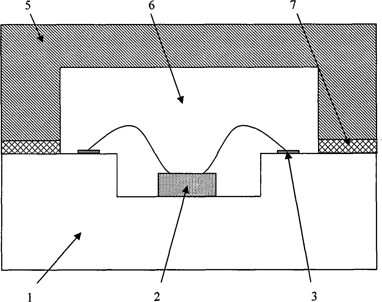
[0054] Low temperature co-fired ceramics are used as substrates, and MEMS devices are vacuum packaged by welding ring sealing method (see image 3 ),
[0055] The steps are:
[0056] 1. According to the needs of MEMS devices, design the interconnection lead structure and the position of various passive components (such as capacitors, inductors, resistors, filters, balanced / unbalanced devices, duplexers, antenna switches, resonant cavities, etc.);
[0057] 2. Put the raw porcelain material of each layer of low-temperature co-fired ceramics into the punching machine, and make via holes and cavities by punching;
[0058] 3. Use stainless steel as a mask on each layer of raw porcelain material, and print metal as interconnection wiring and via filling by mask printing, and braze the passive components at the designated positions;
[0059] 4. The multi-layer raw porcelain material adopts the method of positioning holes for precise lamination and alignment, deglue at a temperature...
Embodiment 3
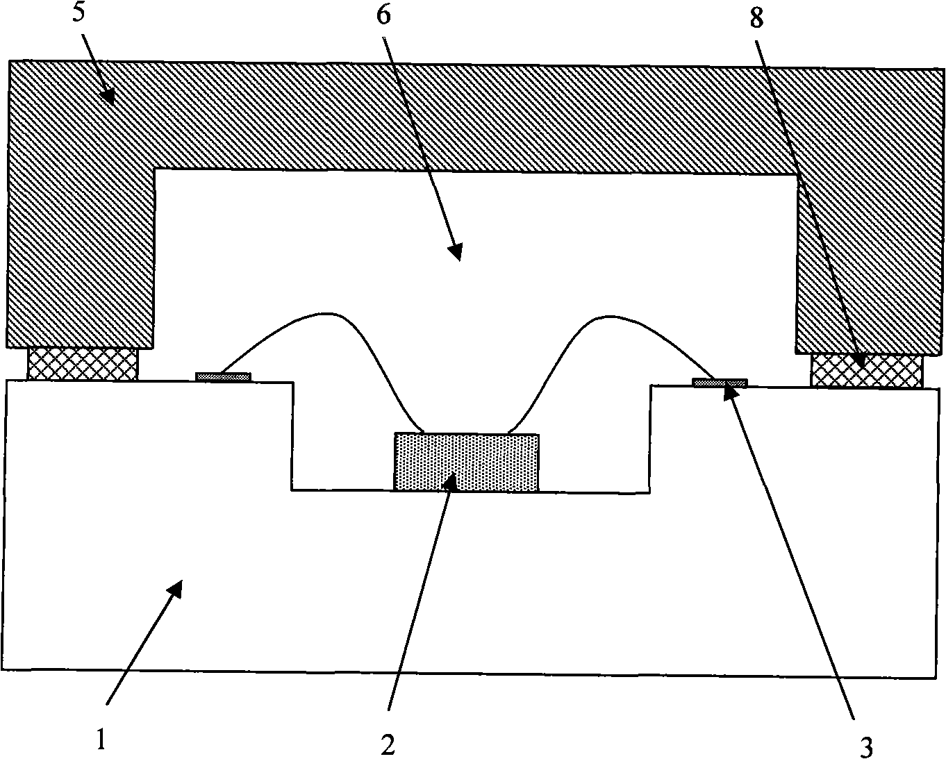
[0067] The low temperature co-fired ceramics are used as the substrate, and the MEMS device is vacuum-packaged by a metal tube sealing method (see Figure 4 ), the steps are:
[0068] 1. According to the needs of MEMS devices, design the interconnection lead structure and the position of various passive components (such as capacitors, inductors, resistors, filters, balanced / unbalanced devices, duplexers, antenna switches, resonant cavities, etc.);
[0069] 2. Put the raw porcelain material of each layer of low-temperature co-fired ceramics into the punching machine, and make via holes and cavities by punching;
[0070] 3. Use stainless steel as a mask on each layer of raw porcelain material, and print metal as interconnection wiring and via filling by mask printing, and braze the passive components at the designated positions;
[0071] 4. The multi-layer raw porcelain material adopts the method of positioning holes for precise lamination and alignment, deglue at a temperature...
PUM
 Abstract
Description
Claims
Application Information