Full forbidden region three-dimensional photon crystal stamp molding method and full forbidden region three-dimensional photon crystal structure

A photonic crystal, bandgap technology, applied in optics, optomechanical equipment, instruments, etc., to achieve high flexibility, elimination of internal defects, and fewer internal defects

Inactive Publication Date: 2008-11-12
XI AN JIAOTONG UNIV
View PDF0 Cites 15 Cited by
  • Summary
  • Abstract
  • Description
  • Claims
  • Application Information

AI Technical Summary

Problems solved by technology

However, the above-mentioned processing methods all have some shortcomings, and can

Method used


Image

  • Full forbidden region three-dimensional photon crystal stamp molding method and full forbidden region three-dimensional photon crystal structure
  • Full forbidden region three-dimensional photon crystal stamp molding method and full forbidden region three-dimensional photon crystal structure
  • Full forbidden region three-dimensional photon crystal stamp molding method and full forbidden region three-dimensional photon crystal structure

Examples


Embodiment Construction

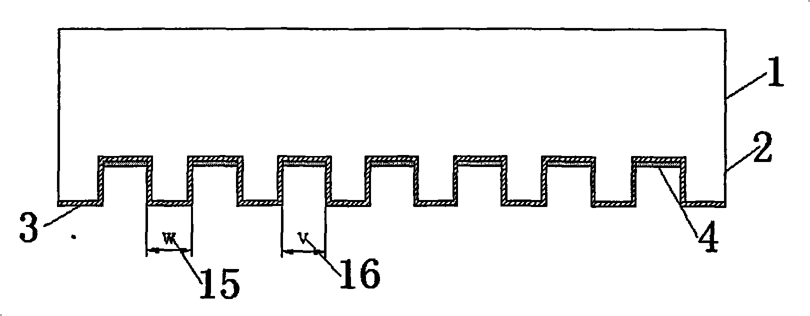
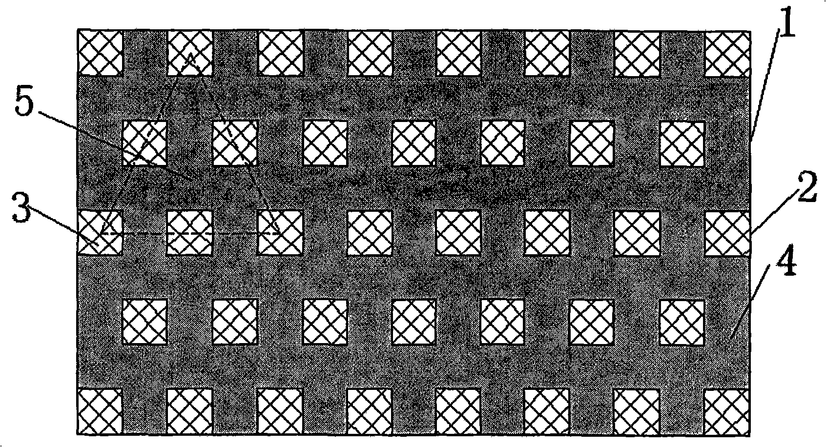
[0029] In the following, the nanoimprint manufacturing method of the total forbidden band three-dimensional photonic crystal will be described in detail in combination with the accompanying drawings.

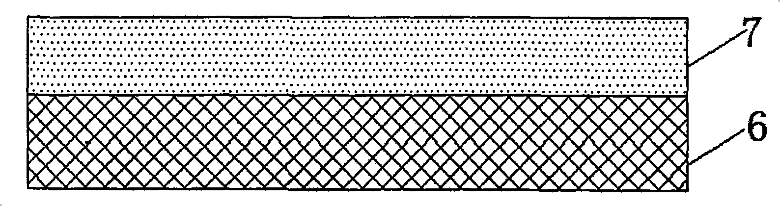
[0030] The full-gap three-dimensional photonic crystal is a three-dimensional photonic crystal with a face-centered cubic structure formed by embedding monodisperse colloidal particles 8 in a polymer matrix material 7 after solidification.

[0031] The basic working principle of the present invention is: select suitable material, select polystyrene as the monodisperse colloid particle, select silicon rubber as the polymer matrix material; Methyl acrylate. A dielectric constant ratio greater than 2 is generated between the monodisperse colloidal particles and the polymer matrix material. At the same time, monodisperse colloidal particles form a face-centered cubic structure in three-dimensional space, and these two points meet the physical conditions for photonic crystals to pro...


PUM


Abstract

The invention relates to the technical field of micro-nano manufacturing, introducing a manufacturing method of a full forbidden-band three-dimensional photonic crystal which is molded through impressing and full forbidden-band three-dimensional photonic crystal structure. The manufacturing method takes polymer silicone rubber or polymethyl methacrylate as base material, adopts the method of nano-imprint to fill monodisperse colloidal particles (such as polystyrene, titanium dioxide or silica) in the polymer base material, causing the monodisperse colloidal particles in the polymer base material to form face-centered cubic structure. The monodisperse colloidal particles are adsorbed in raised part of an impressing template, and micro-contacting type nano-imprint technique is adopted to cause monodisperse colloidal particles in the base material of liquid polymer to form two-dimension structure with the 111 surface of a face-centered cube, wherein, the monodisperse colloidal particles are the element on the 111 surface of the face-centered cube and then the particles on the surface are accumulated layer by layer to finally form the full forbidden-band three-dimensional photonic crystal with the face-centered cubic structure.

Description

technical field [0001] The invention belongs to the technical field of micro-nano manufacturing, and relates to an embossing manufacturing method of a three-dimensional photonic crystal with a total forbidden band and a three-dimensional photonic crystal structure with a total forbidden band. Background technique [0002] Photonic crystals can be divided into one-dimensional, two-dimensional and three-dimensional photonic crystals according to the distribution of their dielectric constant in space. The structure of a three-dimensional photonic crystal includes the geometric configuration of the crystal and the filling ratio of the medium. Common crystal geometries include face-centered cubic, body-centered cubic, and close-packed hexagonal structures. Among them, the face-centered cubic structure is most conducive to obtaining a complete photonic band gap. Three-dimensional photonic crystals are currently manufactured in two basic ways. One is a top-down processing method...

Claims


Application Information

Patent Timeline
IPC IPC(8): G03F7/00
Inventor 刘洪忠丁玉成李欣蒋维涛连芩卢秉恒
Owner XI AN JIAOTONG UNIV
Why Eureka
Try Eureka