Supercharge Your Innovation With Domain-Expert AI Agents!

Operation of photolithography process

A technology of photolithography process and photoresist layer, applied in the field of photolithography process

Active Publication Date: 2011-06-22
TAIWAN SEMICON MFG CO LTD
View PDF0 Cites 0 Cited by
  • Summary
  • Abstract
  • Description
  • Claims
  • Application Information

AI Technical Summary

Problems solved by technology

[0005] The technical problem to be solved by the present invention is to provide a method for carrying out a photolithography process with a chemical cleaning step to solve the problem of water caused by the cleaning step in the photolithography process marks, and improve the problem of patterned photoresist structure line edge roughness

Method used


Image

  • Operation of photolithography process
  • Operation of photolithography process
  • Operation of photolithography process

Examples


Embodiment Construction

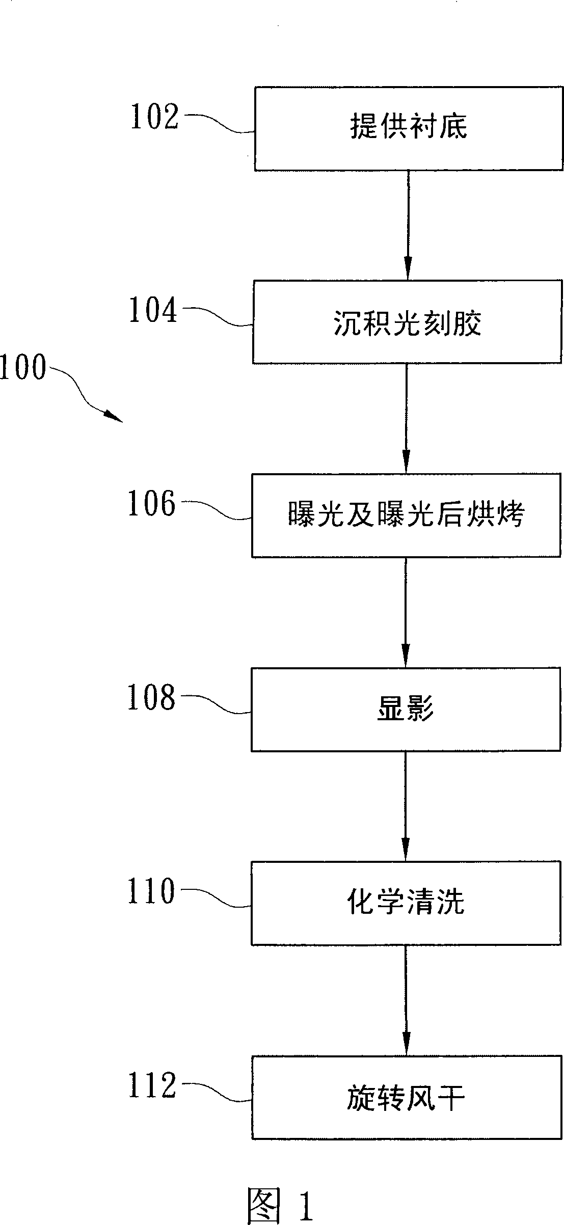
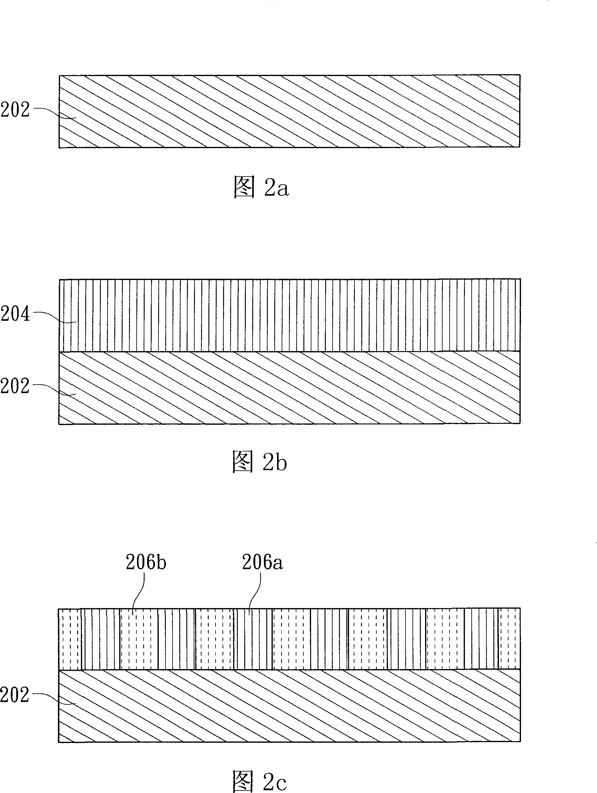
[0028] Step 104 of method 100 is to deposit photoresist on the substrate. refer to Figure 2b , a layer of photoresist 204 is deposited on the substrate 202 . The substrate 202 may include multiple layers of thin films, such as a thin film stack. Photoresist 204 may comprise a conventional photoresist layer and may be deposited on substrate 202 by conventional methods, such as spin-on coating. According to one embodiment of the present invention, the photoresist 204 comprises a conventionally acceptable 193nm photoresist material.

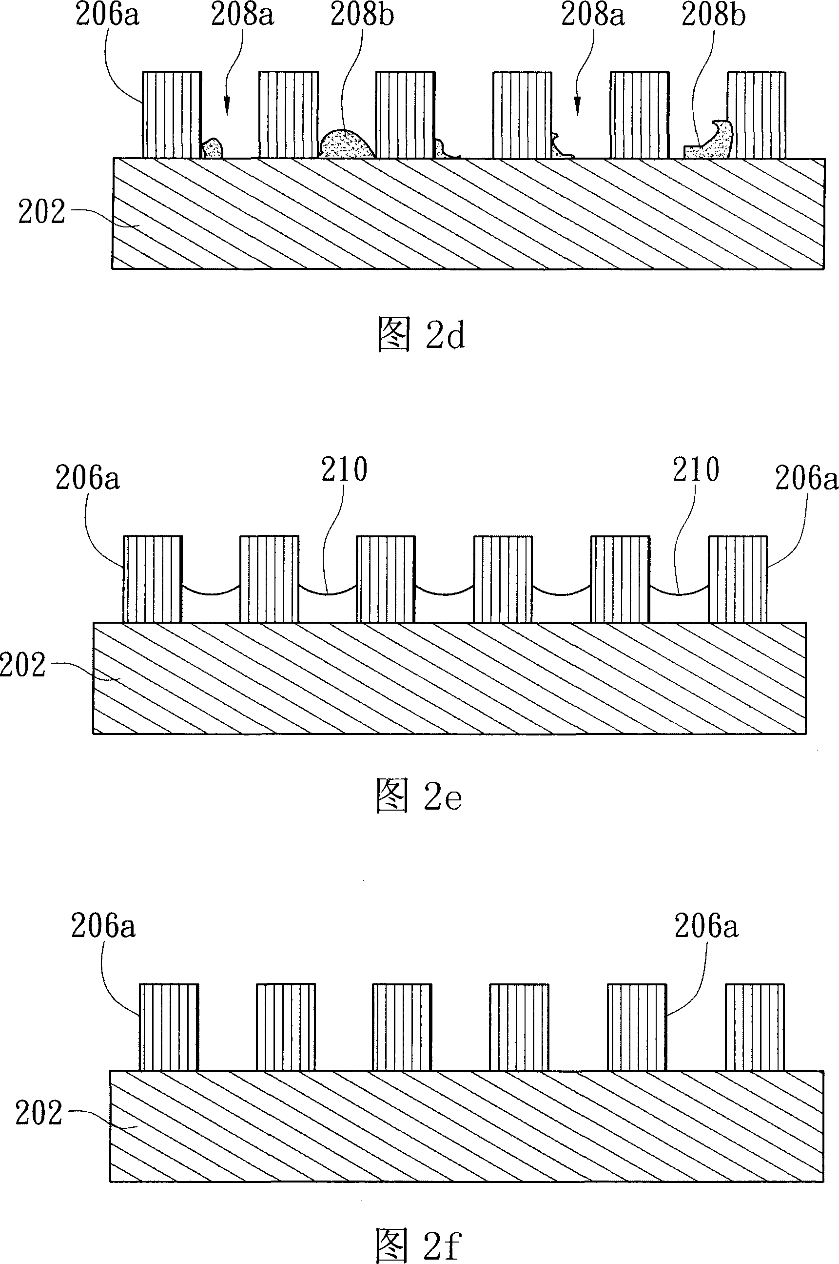
[0029] In step 106, an exposure operation and a post-exposure baking process are performed. refer to Figure 2c , the photoresist 204 is patterned to include exposed photoresist portions 206b and unexposed photoresist portions 206a. It should be understood that different photoresist materials can be used, and a positive photoresist is used as an example for illustration. The exposure system and the baking system may be separate systems.

[0...


PUM


Abstract

The invention discloses a method of performing a lithography process. In one embodiment of the invention, a substrate including a layer of photoresist is provided. The layer of photoresist is exposed. A first chemical rinse solution is applied to the exposed photoresist layer. The first chemical rinse solution includes a first alcohol base chemical. The exposed layer of photoresist is developed. A second chemical rinse solution is applied to the developed photoresist layer. The second chemical rinse solution includes a second alcohol base chemical. The substrate is spun dry after the application of the second chemical rinse solution.

Description

technical field [0001] The invention relates to a photolithography process for manufacturing semiconductor integrated circuits, and in particular to a method for carrying out the photolithography process with chemical cleaning steps. Background technique [0002] Photolithography is a technique for projectively transferring a pattern on a mask onto a substrate such as a semiconductor wafer. The semiconductor photolithography technology includes covering a photoresist layer on the surface of a semiconductor substrate and exposing the photoresist layer to form a pattern. A post-exposure bake process (post-exposure bake; PEB) is usually used to break the polymer structure of the photoresist after exposure. Then the substrate is sent into the developing reaction chamber, the surface of the substrate contains interrupted polymer photoresist, and the photoresist material dissolved in the aqueous developing solution is removed in the reaction chamber with the aqueous developing s...

Claims


Application Information

Patent Timeline
Patent Type & Authority Patents(China)
IPC IPC(8): H01L21/027G03F7/26G03F7/30
CPCG03F7/40G03F7/38
Inventor 张庆裕林进祥
Owner TAIWAN SEMICON MFG CO LTD
Features
  • R&D
  • Intellectual Property
  • Life Sciences
  • Materials
  • Tech Scout
  • Unparalleled Data Quality
  • Higher Quality Content
  • 60% Fewer Hallucinations
Learn More