Optical band artificial composite structure material made by AAO template

A technology of artificial composite and structural materials, applied in the fields of nanostructure manufacturing, nanotechnology, nanotechnology, etc., to achieve the effects of easy mass production, short processing cycle and low cost

Inactive Publication Date: 2008-11-19
INST OF OPTICS & ELECTRONICS - CHINESE ACAD OF SCI
View PDF0 Cites 14 Cited by
  • Summary
  • Abstract
  • Description
  • Claims
  • Application Information

AI Technical Summary

Problems solved by technology

[0005] The technical problem to be solved by the present invention is: aiming at the limitations of the existing microfabrication equipment, a method is proposed to utilize the high order of the AAO template on the nanometer scale to fabricate a double-layer metal structure with a characteristic size in the nanoscale Method for Precisely Aligned Optical Band Surface Plasmon Artificial Composite Structure Materials

Method used


Image

  • Optical band artificial composite structure material made by AAO template
  • Optical band artificial composite structure material made by AAO template
  • Optical band artificial composite structure material made by AAO template

Examples


Embodiment Construction

[0033] The present invention will be described in detail below in conjunction with the accompanying drawings and specific embodiments. But the following examples are only limited to explain the present invention, and the protection scope of the present invention should include the whole content of claim, and promptly can realize the whole content of claim of the present invention to those skilled in the art through following embodiment.

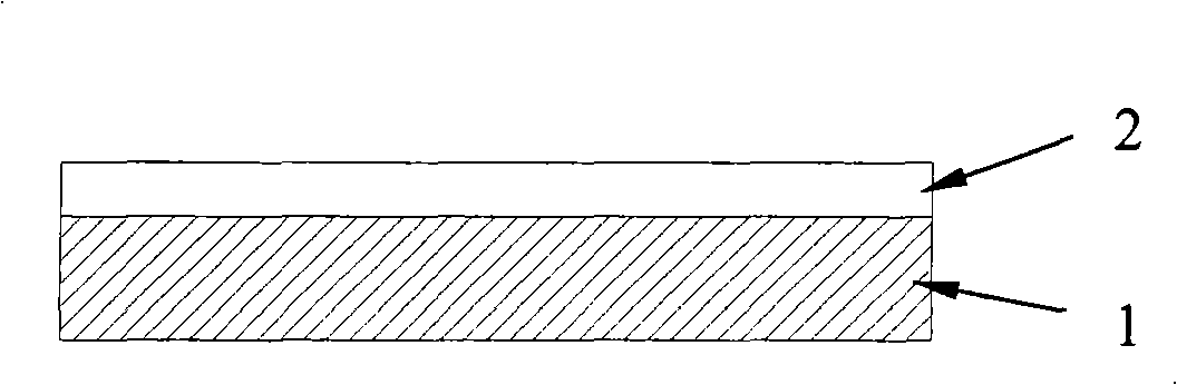
[0034] Such as figure 1 Shown, the schematic diagram of making the first step of the present invention; at first select a piece of silicon substrate 1, and its surface is polished, then sputter-deposits a layer of high-purity aluminum film with a thickness on the order of microns on the polished silicon substrate 1 surface 2;

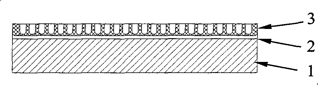
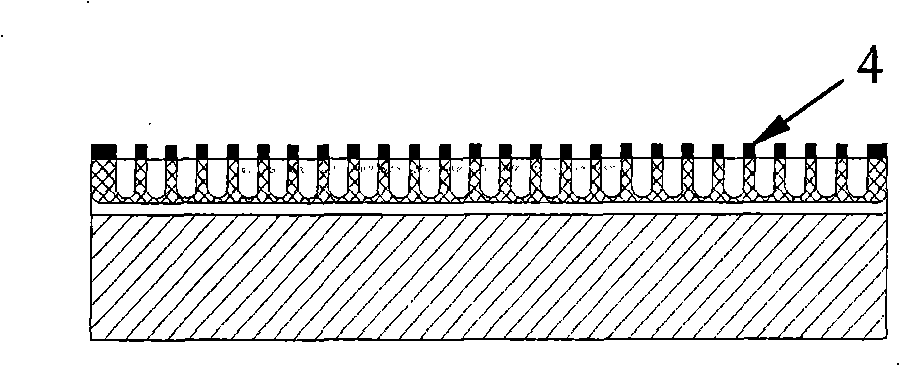
[0035] Such as figure 2 Shown, the production schematic diagram of the second step of the present invention; Adopt electrochemical two-step anodic oxidation method on the surface of high-purity aluminum membrane 2, ...


PUM

PropertyMeasurementUnit
thicknessaaaaaaaaaa

Abstract

A method for preparing optical band artificial composite structural materials by using an AAO template comprises the steps of selecting a polishing optical silicon chip, and depositing a layer of micrometer-grade aluminum film on the surface of the polishing optical silicon chip; preparing a porous alumina template with thickness less than 1 micrometer on the surface of the aluminum film by using an electrochemistry two-step anodic oxidation method; generating a single-channel nano-pore array AAO template; depositing a metal film layer on the single-channel nano-pore array AAO template by using a lateral vacuum deposition method; selecting an optical material substrate, and connecting one surface of the nano-pore array AAO template having the metal film layer with the substrate; removing the silicon chip; eroding the metallic aluminum film layer and the alumina barrier layer at the back side to form a two-channel pore array AAO template; and depositing a metal film layer on the other surface of the AAO template by using the lateral vacuum deposition method. The inventive method has the advantages of low cost, short processing cycle, large processing pattern area, and precise implementation of nanometer grade alignment between an upper metal grid layer and a lower metal grid layer; and has wide application prospect in fundamental research and practical applications of optical band artificial composite structural materials.

Description

technical field [0001] The present invention relates to the production of optical band artificial composite structural materials, in particular to a method for producing optical band artificial composite structural materials by using the highly ordered nature of AAO templates on the nanometer scale. technical background [0002] Surface plasmon artificial composite structure materials in the visible light band mainly use the surface plasmon polaritons (surface plasmonpolaritions, SPPs) effect to modulate the spatial distribution of the amplitude and phase of the light field. By changing the (sub-wavelength) periodic structure parameters of the metal surface, the interaction between SPPs and the light field can be modulated, thereby realizing the artificial manipulation of light propagation. The artificial composite structure materials of surface plasmons in the light band have broad application prospects, for example, It is used in making various SPPs components and circuits...

Claims


Application Information

Patent Timeline
Patent Type & Authority Applications(China)
IPC IPC(8): B82B3/00
Inventor 赵泽宇崔建华史浩飞罗先刚杜春雷
Owner INST OF OPTICS & ELECTRONICS - CHINESE ACAD OF SCI
Why Eureka
Try Eureka