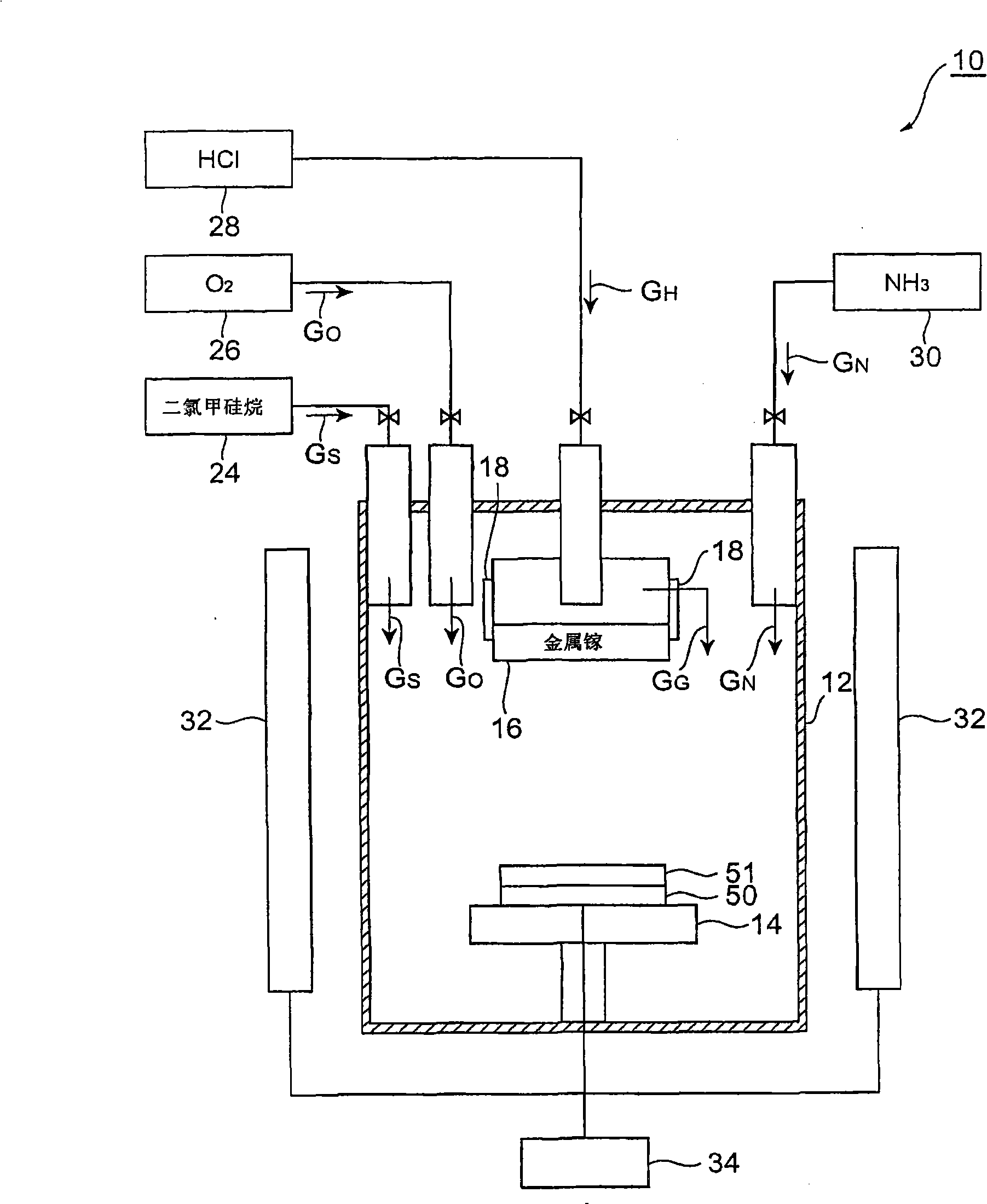
Gallium nitride substrate and gallium nitride film deposition method
A technology of gallium nitride substrate and gallium nitride film, applied in chemical instruments and methods, from chemically reactive gases, crystal growth, etc., can solve the problem of gallium nitride crystals being fragile, increasing the incidence of cracks, defects, etc. problem, to achieve the effect of reducing the incidence of cracking
- Summary
- Abstract
- Description
- Claims
- Application Information
AI Technical Summary
Problems solved by technology
Method used
Image

Examples
Embodiment 1
[0084] Although the present invention is more specifically described below based on examples, the present invention is not limited to the following examples.
[0085] 6 is a table showing test results when GaN layers were formed in Reference Examples 1-1 and 1-2 and Examples 1-1 to 2-4.
[0086] Reference example 1-1
[0087] First, at the growth temperature (T 0 ) is 1100℃, it will have 3.0×10 17 cm -3 A GaN layer with a silicon concentration of 50.8 mm in diameter is grown onto a GaN substrate with a diameter of 50.8 mm. After growth, the GaN layer was annealed for 6 minutes while the temperature was decreased from 1100°C to 500°C at a ramp rate of 100°C / min.
[0088] The surface of the GaN layer was made as a surface obtained by inclining the normal to the (0001) plane by 0.01° in the direction and by 0.01° in the direction. The dislocation density of the GaN layer returns to 5.0×10 7 cm -2 .
[0089] The carrier concentration in the GaN layer is 1×10 17 cm -3 (...
Embodiment 1-1 to 1-10
[0093] In Examples 1-1 to 1-10, the ramp-down temperature was changed for GaN layers having two kinds of silicon concentrations, and the GaN layers were tested.
[0094] In Example 1-1, the GaN layer was formed as in Reference Example 1-1, except that the ramp rate was 50° C. / minute, and the annealing time was 12 minutes. The carrier concentration, activation rate and yield are shown in Figure 6.
[0095] In Examples 1-2 to 1-10, the GaN layer was formed in the same manner as in Example 1-1, except that the silicon concentration, ramp rate, and annealing time were appropriately changed. The carrier concentration, activation rate and yield are shown in Figure 6.
Embodiment 2-1 to 2-4
[0097] In Examples 2-1 to 2-4, the growth temperature (T 0 ), and the GaN layer was tested.
[0098] In Example 2-1, in addition to the growth temperature (T 0 ) was 1050° C. and the annealing time was 11 minutes, a GaN layer was formed in a similar manner to Example 1-1. The carrier concentration, activation rate and yield are shown in Figure 6.
[0099] In Examples 2-2 to 2-4, in addition to appropriately changing the silicon concentration, the growth temperature (T 0 ) and annealing time, a GaN layer was formed in a similar manner to Example 2-1. The carrier concentration, activation rate and yield are shown in Figure 6.
PUM
| Property | Measurement | Unit |
|---|---|---|
| thickness | aaaaa | aaaaa |
| diameter | aaaaa | aaaaa |
| thickness | aaaaa | aaaaa |
Abstract
Description
Claims
Application Information
 - R&D
- Intellectual Property
- Life Sciences
- Materials
- Tech Scout
- Unparalleled Data Quality
- Higher Quality Content
- 60% Fewer Hallucinations
Browse by: Latest US Patents, China's latest patents, Technical Efficacy Thesaurus, Application Domain, Technology Topic, Popular Technical Reports.
© 2025 PatSnap. All rights reserved.Legal|Privacy policy|Modern Slavery Act Transparency Statement|Sitemap|About US| Contact US: help@patsnap.com