Nanocrystalline floating gate structure non-volatility memory cell and its manufacture method

A non-volatile storage, nanocrystalline technology, applied in the field of microelectronics, can solve the problems of poor feasibility and compatibility, difficult process control, complex manufacturing process, etc., and achieve the effect of improving service life, simple structure and manufacturing process, and cost saving.

Inactive Publication Date: 2008-11-26
INST OF MICROELECTRONICS CHINESE ACAD OF SCI
View PDF18 Cites 13 Cited by
  • Summary
  • Abstract
  • Description
  • Claims
  • Application Information

AI Technical Summary

Problems solved by technology

However, the preparation of nanocrystals by the above methods generally has the disadvantages of complex manufacturing process, high manufacturing cost, low manufacturing efficiency, or difficult process control during the manufacturing process, or poor feasibility and poor compatibility with traditional CMOS processes.

Method used


Image

  • Nanocrystalline floating gate structure non-volatility memory cell and its manufacture method
  • Nanocrystalline floating gate structure non-volatility memory cell and its manufacture method
  • Nanocrystalline floating gate structure non-volatility memory cell and its manufacture method

Examples


Embodiment Construction

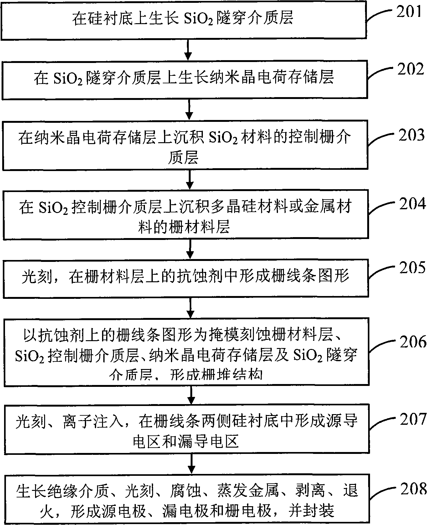
[0071]In order to make the object, technical solution and advantages of the present invention clearer, the present invention will be described in further detail below in conjunction with specific embodiments and with reference to the accompanying drawings.

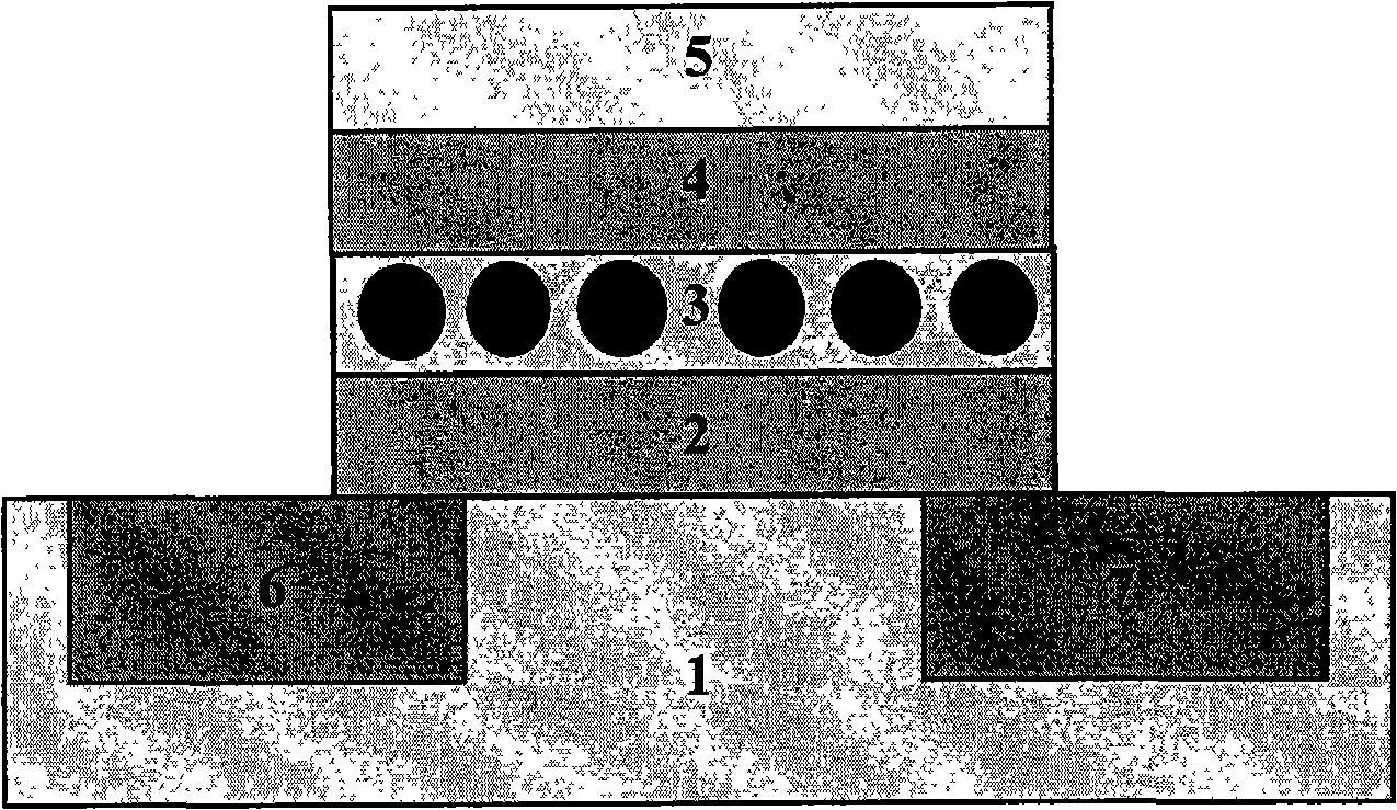
[0072] Such as figure 1 as shown, figure 1 The structure diagram of the non-volatile storage unit of the nanocrystalline floating gate structure provided by the present invention, the non-volatile storage unit of the floating gate structure includes: a silicon substrate 1, heavily doped source conductors located on both sides of the silicon substrate 1 The region 6 and the drain conduction region 7, the tunnel dielectric layer 2 covering the carrier channel between the source conduction region 6 and the drain conduction region 7, the nanocrystalline charge storage layer 3 covering the tunnel dielectric layer, covering the A control gate dielectric layer 4 on the nanocrystalline charge storage layer and a gate material lay...


PUM


Abstract

The invention relates to the micro-electronics technical field, and discloses a non-volatile storage unit of a nanocrystal floating gate structure, which comprises a silicon substrate, a source conduction region 6, a drain conduction region 7, a tunneling dielectric layer 2, a nanocrystal charge storage layer 3, a control gate dielectric layer 4 and a gate material layer 5, wherein the source conduction region 6 and the drain conduction region 7 which are heavily doped are arranged on two ends of the silicon substrate 1, the tunneling dielectric layer 2 is covered on a current carrier channel between the source conduction region 6 and the drain conduction region 7, the nanocrystal charge storage layer is covered on the tunneling dielectric layer, the control gate dielectric layer 4 is covered on the nanocrystal charge storage layer, and the gate material layer 5 is covered on the control gate dielectric layer. The invention simultaneously discloses a process for preparing the non-volatile storage unit of a nanocrystal floating gate structure. The non-volatile storage unit of a nanocrystal floating gate structure increases programming/erasing speed of the non-volatile storage unit of a floating gate structure, effective storage capacity, data retention, programming/erasing durability and the like, and the process for preparing the non-volatile storage unit of a nanocrystal floating gate structure simplifies manufacturing technique, increases manufacturing efficiency and reduces manufacturing cost based on the conventional CMOS technique.

Description

technical field [0001] The invention relates to the technical field of microelectronics, in particular to a non-volatile storage unit with a nanocrystal floating gate structure and a manufacturing method thereof. Background technique [0002] Floating gate structure memory is a mainstream memory type widely used and generally recognized at present. It is a very important semiconductor component and is widely used in the electronics and computer industries. Due to its own structure and material selection, the traditional floating gate memory cell requires fast write / erase operations and long-term high-stable storage performance, and this contradiction does not change with the reduction of feature size. Obvious improvements have been made, limiting the development of floating gate memory cells. [0003] As the feature size enters the nanoscale, how to adapt to the development of the process and improve the performance of writing, reading, erasing and maintaining the stored da...

Claims


Application Information

Patent Timeline
Patent Type & Authority Applications(China)
IPC IPC(8): H01L29/788H01L29/49H01L27/115H01L21/336H01L21/28H01L21/8247
Inventor 胡媛刘明龙世兵杨清华管伟华李志刚刘琦
Owner INST OF MICROELECTRONICS CHINESE ACAD OF SCI
Why Eureka
Try Eureka