Method for improving medium layer defect between micro-reflection mirrors and producing silicon based LCD

A technology of micro-mirror and dielectric layer, which is applied in the direction of equipment, photo-plate making process of patterned surface, optics, etc., can solve the problems of reducing the reflectivity of micro-mirror, affecting the quality of micro-mirror, etc., and achieve the increase of opening width, Effect of reducing diffuse reflection and increasing reflectivity

Inactive Publication Date: 2008-12-03
SEMICON MFG INT (SHANGHAI) CORP
View PDF1 Cites 3 Cited by
  • Summary
  • Abstract
  • Description
  • Claims
  • Application Information

AI Technical Summary

Problems solved by technology

[0010] In the prior art, due to the residual dielectric layer sidewall on the metal layer connected to the groove, the micro-mirror surface produces diffuse reflection, which reduces the reflectivity of the micro-mirror, thereby affecting the quality of the micro-mirror

Method used


Image

  • Method for improving medium layer defect between micro-reflection mirrors and producing silicon based LCD
  • Method for improving medium layer defect between micro-reflection mirrors and producing silicon based LCD
  • Method for improving medium layer defect between micro-reflection mirrors and producing silicon based LCD

Examples


Embodiment Construction

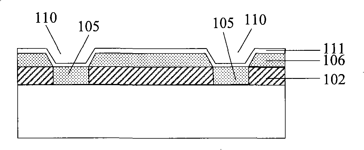
[0022] The invention performs acid etching on the dielectric layer, so that the opening aspect ratio of the dielectric layer at the trench is increased, that is, the opening width is increased, and no insulating dielectric is produced on the metal layer connected to the trench in the subsequent etching process. The layered side wall reduces the diffuse reflection of the micro-mirror and improves the reflectivity of the micro-mirror.

[0023] The specific implementation of the present invention will be described in detail below in conjunction with the accompanying drawings.

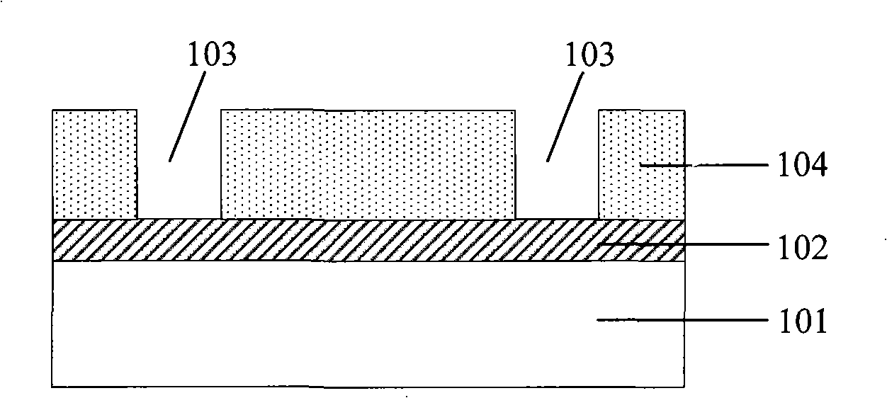
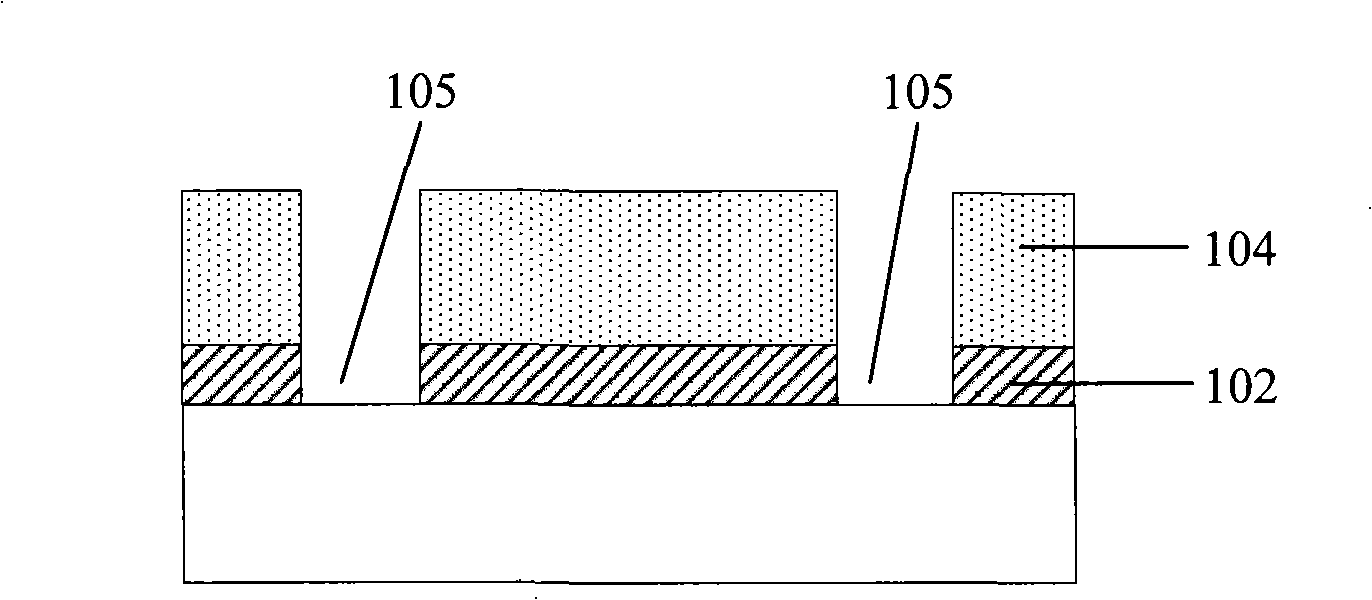
[0024] Figure 6 It is a flow chart of an embodiment of the present invention to improve the defect of the dielectric layer between the micro-mirrors. Such as Figure 6 As shown, step S101 is executed, first, a silicon substrate with a metal layer is provided, and the metal layer includes a trench penetrating the metal layer; step S102 is executed, a dielectric layer is deposited on the metal layer, and ...


PUM

PropertyMeasurementUnit
thicknessaaaaaaaaaa
thicknessaaaaaaaaaa
thicknessaaaaaaaaaa

Abstract

A method for improving defects of medium layer between micro-reflectors comprises the following steps: providing a silicon substrate with a metal layer having a groove penetrating through the metal layer; depositing a medium layer on the metal layer to fill the groove; acid-etching the medium layer; forming a photoresist layer on the medium layer; and etching the photoresist layer and the medium layer until the metal is exposed to form a micro-reflector array. The invention further provides a method for fabricating LCD on silicon. The medium layer is subjected to acid-etching to increase the opening aspect ratio and the opening width of the medium layer at the groove, so that no sidewalls of the medium layer is produced on the metal layer connected with the groove in subsequent etching process, thus reducing diffuse reflection and improving reflectivity of the micro-reflector.

Description

technical field [0001] The invention relates to a manufacturing method of a liquid crystal on silicon (LCOS) display, in particular to a method for improving the defect of a dielectric layer between microreflectors. Background technique [0002] In recent years, many new technologies have emerged in the liquid crystal (LCD) industry, among which the more popular technology is Liquid Crystal on Silicon (LCOS, Liquid Crystal on Silicon) technology. LCOS (LiquidCrystal on Silicon) is a new reflective micro LCD projection technology. Its structure is to grow a transistor on a silicon substrate, use a semiconductor process to make a drive panel (also known as CMOS-LCD), and then grind it on the transistor. The technology is ground and plated with aluminum as a micro-mirror to form a CMOS substrate, and then the CMOS substrate is bonded to the glass substrate containing the transparent electrode, and then the liquid crystal is pumped in for packaging and testing. [0003] Compare...

Claims


Application Information

Patent Timeline
Patent Type & Authority Applications(China)
IPC IPC(8): G02F1/1362G03F7/00
Inventor 向阳辉曾贤成
Owner SEMICON MFG INT (SHANGHAI) CORP
Why Eureka
Try Eureka